

Solar cell and method for manufacturing solar cell
A technology of solar cells and electrodes, applied in the field of solar cells, can solve the problems of limited application range, high cost, difficulty in large-scale, etc.
- Summary
- Abstract
- Description
- Claims
- Application Information
AI Technical Summary
Problems solved by technology
Method used
Image

Examples
Embodiment 1
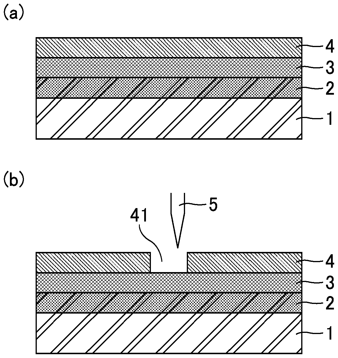
[0139] Aluminum foil (manufactured by UACJ, general-purpose aluminum A1N30 grade, thickness 100μm) was anodized with aluminum sulfate film treatment for 30 minutes to form an aluminum oxide film (thickness 5μm, thickness ratio) on the surface of the aluminum foil 5%) to obtain a flexible substrate.
[0140] Using a batch sputtering device (manufactured by ULVAC), a 6-inch Ti target was formed into a hard film containing titanium nitride (TiN) (with a thickness of 100 nm, dimension Its hardness is 2100HV). At this time, 20sccm of Ar and 5sccm of N are introduced as process gas 2 , Adjust the pressure so that the pressure during film formation reaches 0.1Pa.
[0141] An Al film with a thickness of 100 nm was formed on the hard film by a vapor deposition machine, and a Ti film with a thickness of 100 nm was formed on the Al film by a sputtering method to form a cathode (Ti / Al film). Using a mechanical scribing machine (manufactured by Mitsuboshi Diamond Industrial Co., Ltd., KMPD100...
Embodiment 2~12
[0149] Except having changed the hard film as shown in Table 1, it carried out similarly to Example 1, and obtained the solar cell.
Embodiment 13
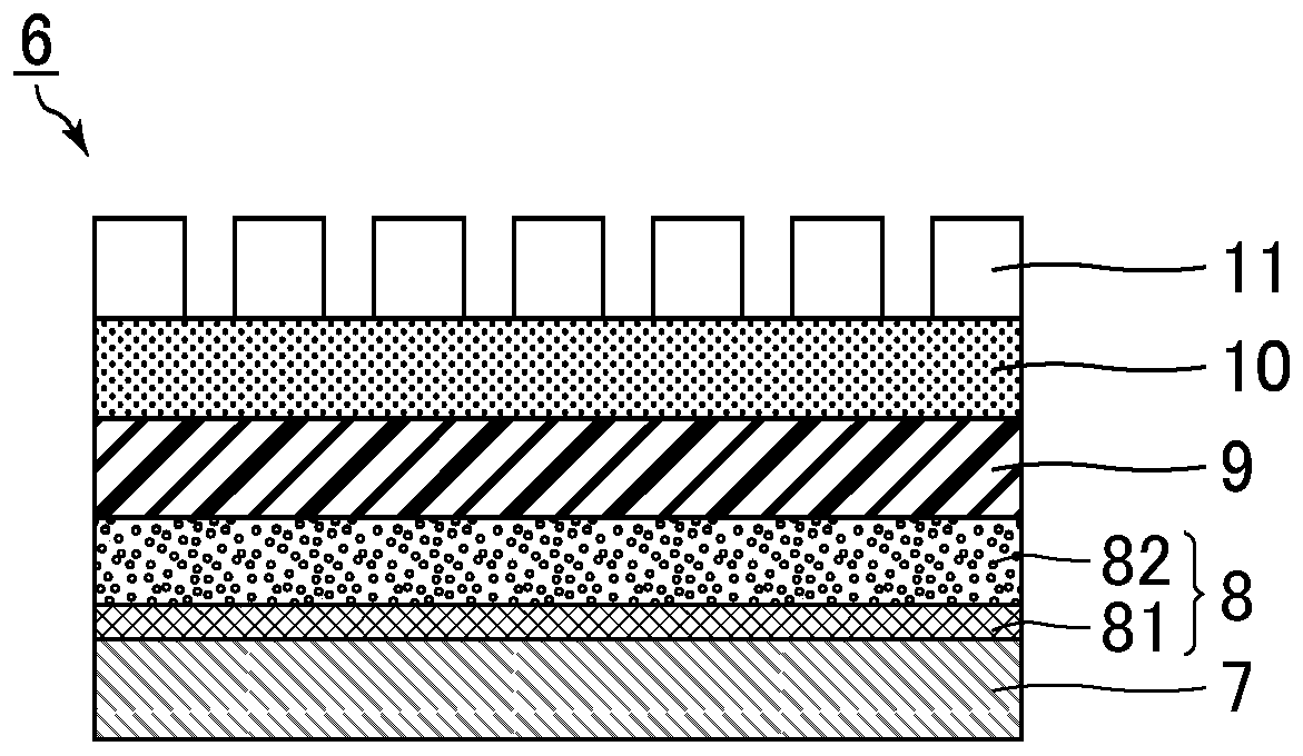
[0164] On the glass substrate, an aluminum film with a thickness of 200 nm as a conductive layer and a molybdenum film with a thickness of 50 nm as a cathode were successively formed by the electron beam evaporation method.
[0165] Next, using a sputtering device (manufactured by ULVAC), titanium oxide was sputtered on the surface of the cathode, thereby forming a thin-film electron transport layer with a thickness of 30 nm. Furthermore, an ethanol dispersion of titanium oxide (a mixture of 10 nm and 30 nm in average particle diameter) was coated on the thin-film electron transport layer by spin coating, and then fired at 200°C for 10 minutes to form a porous 150 nm thick Electron transport layer.
[0166] Next, as a solution for forming an organic-inorganic perovskite compound, N,N-dimethylformamide (DMF) was used as a solvent, and CH 3 NH 3 I and PbI 2 Dissolve at a molar ratio of 1:1, the CH 3 NH 3 I and PbI 2 The total weight concentration is adjusted to 20%. This solution wa...
PUM
| Property | Measurement | Unit |
|---|---|---|
| Vickers hardness | aaaaa | aaaaa |
| Vickers hardness | aaaaa | aaaaa |
| thickness | aaaaa | aaaaa |
Abstract
Description
Claims
Application Information