Long-working distance plasmon nanolithography method

A working distance and plasmon technology, applied in the field of lithography, can solve the problems of shallow exposure depth, limited exposure distance, and limited wide application, etc., and achieve the effects of high resolution, extended exposure distance, and extended exposure depth.

Inactive Publication Date: 2019-10-08
UNIV OF SCI & TECH OF CHINA
View PDF1 Cites 2 Cited by
  • Summary
  • Abstract
  • Description
  • Claims
  • Application Information

AI Technical Summary

Problems solved by technology

However, the rapid divergence of the light field leads to two disadvantages in plasmonic nanolithography: (1) the exposure distance is limited, that is, the contact between the metal template and the photosensitive layer is tight (<5nm); (2) the exposure depth (depth of focus ) shallow (5 ~ 10nm)
This near-field lithography method severely limits the wide application of the technology

Method used


Image

  • Long-working distance plasmon nanolithography method
  • Long-working distance plasmon nanolithography method
  • Long-working distance plasmon nanolithography method

Examples


preparation example Construction

[0043] A) prepare bow tie photolithography head, the preparation method of described bow tie photolithography head comprises:

[0044] a-1) depositing an aluminum film on the first substrate;

[0045] a-2) using a focused ion beam to etch a bow tie structure on the aluminum film as the exposure aperture;

[0046] a-3) spin coating PMMA layer on the aluminum film;

[0047] a-4) depositing the first silver film layer on the PMMA layer to obtain the bow tie lithography head;

[0048] B) prepare exposure substrate, the preparation method of described exposure substrate comprises:

[0049] b-1) depositing a second silver film on a second substrate;

[0050] b-2) spin-coating the photoresist layer on the second silver film to obtain an exposure substrate;

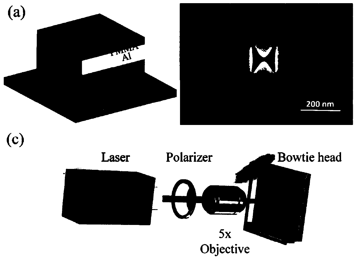
[0051] C) the bow tie lithography head is in close contact with the exposure substrate, that is, the first silver film layer of the bow tie lithography head is in close contact with the photoresist layer of the exposure subst...

Embodiment 1

[0105] 1) Preparation of "bow tie lithography head"

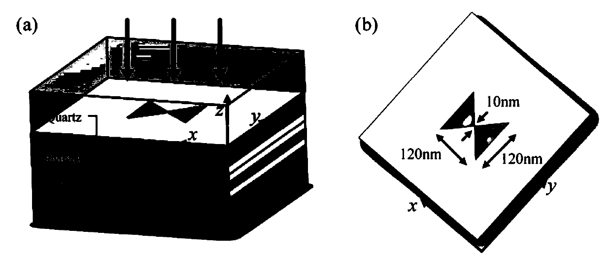
[0106] a) Using the chromium layer (sputter coating, 100nm) as a mask, the step structure on the quartz substrate was obtained by wet etching (as attached figure 2 shown), its typical size is 300 μm × 300 μm × 50 μm.

[0107] b) On the basis of the above steps, deposit an aluminum layer (sputter coating, 100nm) on the substrate;

[0108] c) On the basis of the above steps, use focused ion beam (focus ion beam, FIB) to etch a bow tie structure on the aluminum film as the exposure aperture, the typical size of which is 120nm×120nm, and the distance between the sharp corners of the aperture is 10nm;

[0109] D) on the basis of the above steps, spin coat the PMMA layer (20nm) on the aluminum film;

[0110] e) On the basis of the above steps, deposit the first silver layer (sputter coating, 20nm) on the PMMA layer.

[0111] 2) "Exposure substrate" preparation

[0112] a) preparing the substrate (such as a silicon substrate)...

Embodiment 2

[0128] 6) Preparation of "bow tie lithography head"

[0129] f) Using the chromium layer (sputter coating, 100nm) as a mask, obtain the step structure on the quartz substrate by wet etching (as attached figure 2 shown), its typical size is 300 μm × 300 μm × 50 μm.

[0130] g) On the basis of the above steps, deposit an aluminum layer (sputter coating, 100nm) on the substrate;

[0131] h) On the basis of the above steps, use focused ion beam (focus ion beam, FIB) to etch a bow tie structure on the aluminum film as the exposure aperture, the typical size of which is 120nm×120nm, and the distance between the sharp corners of the aperture is 10nm;

[0132] i) on the basis of the above steps, spin coat the PMMA layer (20nm) on the aluminum film;

[0133] j) On the basis of the above steps, deposit a first silver layer (sputter coating, 20 nm) on the PMMA layer.

[0134] 7) "Exposure substrate" preparation

[0135] e) preparing a substrate (such as a silicon dioxide substrate);...


PUM

PropertyMeasurementUnit
thicknessaaaaaaaaaa
thicknessaaaaaaaaaa
thicknessaaaaaaaaaa

Abstract

The invention provides a long-working distance plasmon nanolithography method. The method comprises steps: A) a bowtie lithography head is prepared; B) an exposure substrate is prepared; C) the bowtielithography head is closely contacted with the exposure substrate, that is, a first silver film layer of the bowtie lithography head is closely contacted with a photoresist layer of the exposure substrate; and D) a laser light source is adopted, through polarizer and objective lens adjustment, an exposure light field parallel with a bowtie-type aperture sharp corner is acquired, and a nanostructure is obtained through exposure and development. In comparison with the prior art, through involving the bowtie-type structure in an aluminum mask, local enhancement on the light field can be realizedto acquire higher resolution; through refractive index match between a silver layer and a PMMA layer, the surface plasmon excitation efficiency can be enhanced, and the exposure distance is prolonged; and a metal-medium-metal structure is formed through a silver layer-photoresist layer-silver layer, focal depth modulation can be realized, and the exposure depth is prolonged.

Description

technical field [0001] The invention relates to the technical field of photolithography, in particular to a long working distance plasmon nanometer photolithography method. Background technique [0002] Lithography is a pattern generation process and a key part of the semiconductor manufacturing process. Photolithography is a photolithography technology widely used in the semiconductor industry. The minimum feature size (resolution) that optical lithography can achieve is mainly determined by the wavelength of the exposure light source and the numerical aperture of the exposure system, which is limited by the diffraction limit. For example, using 193nm ArF excimer laser as the exposure light source, combined with immersion lithography and multiple exposure processes, the optical lithography method can realize the 22nm semiconductor process node. In the case where it is difficult to increase the numerical aperture, higher resolution means that the exposure wavelength must b...

Claims


Application Information

Patent Timeline
Patent Type & Authority Applications(China)
IPC IPC(8): G03F7/00G03F7/20G02B5/00B82Y40/00B82Y10/00B81C99/00B32B37/26
CPCB32B37/26B81C99/009B82Y10/00B82Y40/00G02B5/008G03F7/0002G03F7/0017G03F7/2004G03F7/70058G03F7/7015G03F7/70275G03F7/70325G03F7/70366
Inventor 王亮秦金罗慧雯
Owner UNIV OF SCI & TECH OF CHINA
Why Eureka
Try Eureka