Supercharge Your Innovation With Domain-Expert AI Agents!

Two-dimensional strontium niobate nanosheet ultraviolet phototransistor detector

A technology of nanosheets and strontium niobate, which is applied to semiconductor devices, circuits, electrical components, etc., can solve the problems of slow response speed and large dark current, and achieve the effect of fast response speed and high photoelectric gain

Active Publication Date: 2021-07-23
FUDAN UNIV
View PDF4 Cites 0 Cited by
  • Summary
  • Abstract
  • Description
  • Claims
  • Application Information

AI Technical Summary

Problems solved by technology

At present, many UVA ultraviolet detection materials have shortcomings such as slow response speed and large dark current, while optoelectronic devices are gradually developing in the direction of miniaturization, energy saving, flexible wearable, etc.

Method used


Image

  • Two-dimensional strontium niobate nanosheet ultraviolet phototransistor detector
  • Two-dimensional strontium niobate nanosheet ultraviolet phototransistor detector
  • Two-dimensional strontium niobate nanosheet ultraviolet phototransistor detector

Examples


Embodiment 1

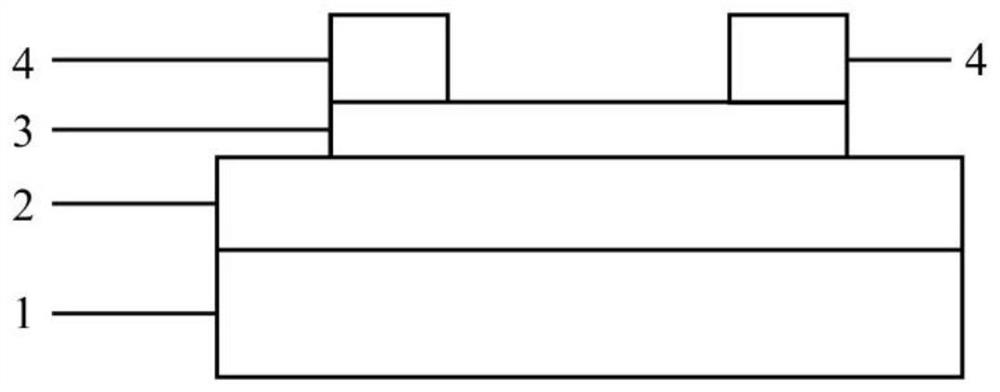
[0027] Embodiment 1, a kind of two-dimensional strontium niobate nanosheet ultraviolet phototransistor detector, such as figure 1 shown, including SiO 2 / Si substrate 1, 2, spin-coated strontium niobate Sr dispersed on the substrate 2 Nb 3 o 10 Nano sheet 3, a chromium-gold electrode 4 in contact with the upper surface of the nano sheet.

Embodiment 2

[0028] The preparation steps of the two-dimensional strontium niobate nanosheet ultraviolet phototransistor detector in this embodiment are as follows:

[0029] (1) Preparation of strontium niobate nanosheets, using high-temperature solid-state reaction-ion exchange-liquid phase exfoliation method: 99.9% pure solid Cs 2 CO 3 , SrCO 3 and Nb 2 o 5 The powder is mixed and ground for 1 hour according to the molar ratio of 1:1.8:2.5, and sintered at a high temperature of 1200°C for 6 hours, and the product is cooled with the furnace. The obtained product was mixed with 1 mol / L hydrochloric acid, ion-exchanged for 5 days, and then the product was washed several times with ultrapure water and dried. A certain amount of the obtained product was weighed, mixed with an equimolar ratio tetrabutylammonium hydroxide (TBAOH) solution, shaken at room temperature for 10 days with a multi-purpose oscillator, and centrifuged to obtain the stripped strontium niobate nanosheets. The product...

Embodiment 2

[0031] Example 2, using the ultraviolet phototransistor detector prepared by the present invention to detect incident light in a specific ultraviolet band:

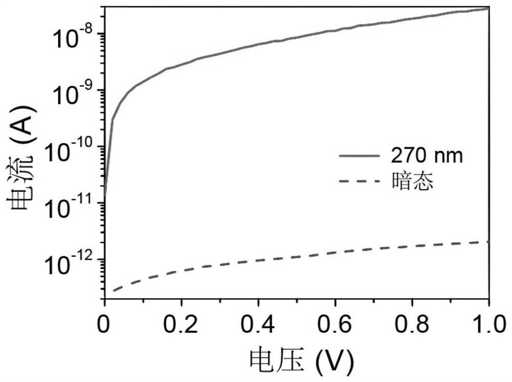
[0032] Utilize the ultraviolet phototransistor detector shown in embodiment 1, device source, drain are connected with semiconductor testing system respectively, change voltage, record the electric current that flows through device under dark state and illumination condition, as image 3 shown. Under the same voltage, the device exhibited a higher current when irradiated with 270nm ultraviolet light.

[0033] Using the ultraviolet phototransistor detector shown in Example 1, connect the source and drain of the device to the semiconductor test system respectively, keep the bias voltage constant, change the wavelength of the incident ultraviolet light, record the current flowing through the device, and calculate the response rate ,Such as Figure 4 shown. The device exhibits good detection performance near the ultraviole...


PUM

PropertyMeasurementUnit
thicknessaaaaaaaaaa
diameteraaaaaaaaaa
thicknessaaaaaaaaaa

Abstract

The invention belongs to the technical field of semiconductor optoelectronic devices, in particular to a two-dimensional strontium niobate nanosheet ultraviolet phototransistor detector. The ultraviolet detector of the present invention comprises: SiO 2 / Si substrate, strontium niobate Sr 2 Nb 3 o 10 Nanosheets and Cr‑Au contact electrodes. where Sr 2 Nb 3 o 10 Nanosheets dispersed on SiO by spin coating 2 On the / Si substrate, the ultraviolet lithography chromium-gold electrode is in contact with the upper surface of the nanosheet to form a back gate ultraviolet phototransistor structure. Two-dimensional strontium niobate nanosheets have a high band gap, which can realize filter-free narrow-band ultraviolet light detection; the distance between the micrometer electrodes is close, and it has high detection rate and photoelectric gain under ultraviolet light irradiation, and the response speed is fast; forming a back gate Polar phototransistor, which can control the carrier concentration of nanosheets by adjusting the gate voltage, has bipolar characteristics under different gate voltages; the side length of the two-dimensional strontium niobate transistor device is only about 200 μm, which is helpful for the miniaturization of the device .

Description

technical field [0001] The invention belongs to the technical field of semiconductor optoelectronic devices, in particular to a two-dimensional strontium niobate nanosheet ultraviolet phototransistor detector. Background technique [0002] In recent years, high-performance ultraviolet detectors have been greatly developed and widely used in spectral analysis, environmental monitoring, optoelectronic devices and other fields. Due to the advantages of simple structure and no need for complicated filtering devices, wide bandgap semiconductors have attracted widespread attention. At present, many UVA ultraviolet detection materials have disadvantages such as slow response speed and large dark current, while optoelectronic devices are gradually developing in the direction of miniaturization, energy saving, flexible and wearable. Two-dimensional perovskite materials have the advantages of high absorbance, adjustable band gap, high transparency of visible light, and good mechanica...

Claims


Application Information

Patent Timeline
Patent Type & Authority Patents(China)
IPC IPC(8): H01L31/0224H01L31/032H01L31/0352H01L31/11H01L31/18
CPCH01L31/022408H01L31/032H01L31/0352H01L31/1105H01L31/18Y02P70/50
Inventor 方晓生李思远
Owner FUDAN UNIV
Features
  • R&D
  • Intellectual Property
  • Life Sciences
  • Materials
  • Tech Scout
  • Unparalleled Data Quality
  • Higher Quality Content
  • 60% Fewer Hallucinations
Learn More