Check patentability & draft patents in minutes with Patsnap Eureka AI!

Gallium nitride HEMT device structure and preparation method thereof

A device structure and gallium nitride technology, applied in the field of microelectronics, can solve the problems of device performance degradation and reliability, and achieve the effects of simple manufacturing process, high breakdown voltage resistance and high breakdown voltage

Inactive Publication Date: 2020-03-06
西安电子科技大学芜湖研究院
View PDF4 Cites 1 Cited by
  • Summary
  • Abstract
  • Description
  • Claims
  • Application Information

AI Technical Summary

Problems solved by technology

However, the serious interface problem between the gate insulating layer and the nitride will cause device performance degradation and reliability problems, which has become a hot spot of international research in recent years

Method used


Image

  • Gallium nitride HEMT device structure and preparation method thereof
  • Gallium nitride HEMT device structure and preparation method thereof

Examples


Embodiment 1

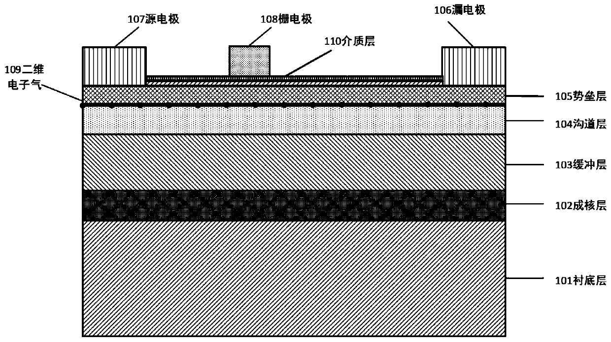
[0033] 1. Use MOCVD technology and equipment to carry out AlGaN / GaN heterojunction epitaxy on a 6-inch substrate (insulating or semi-insulating sapphire, silicon, silicon carbide, gallium nitride, zinc oxide, and diamond, etc.). This technology is a general conventional technology. The AlGaN / GaN heterojunction structure sequentially includes a gallium nitride (GaN) buffer layer 103, a low-temperature gallium nitride (GaN) nucleation layer 102, a gallium nitride (GaN) channel layer 104, an aluminum Gallium nitride (AlGaN) barrier functional layer 105 and a channel 109 of high-concentration two-dimensional electron gas (2DEG) formed at the interface.

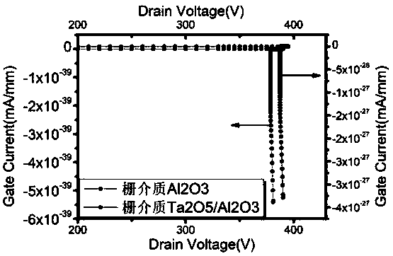
[0034] 2. Deposit Ta on the surface of the above-mentioned AlGaN / GaN heterojunction material by atomic layer deposition (ALD) 2 o 5 Thin film layer with Al 2 o 3 The thin film layer is used as a dielectric layer with a thickness of 50nm.

[0035] 3. Organically clean the material obtained in the previous step. After cleaning, ...

Embodiment 2

[0040] 1. Use MOCVD technology and equipment to carry out AlGaN / GaN heterojunction epitaxy on a 6-inch substrate (insulating or semi-insulating sapphire, silicon, silicon carbide, gallium nitride, zinc oxide, and diamond, etc.). This technology is a general conventional technology. The AlGaN / GaN heterojunction structure sequentially includes a gallium nitride (GaN) buffer layer 103, a low-temperature gallium nitride (GaN) nucleation layer 102, a gallium nitride (GaN) channel layer 104, an aluminum Gallium nitride (AlGaN) barrier functional layer 105 and a channel 109 of high-concentration two-dimensional electron gas (2DEG) formed at the interface.

[0041] 2. Deposit Ta on the surface of the above-mentioned AlGaN / GaN heterojunction material by atomic layer deposition (ALD) 2 o 5 Thin film layer with Al 2 o 3 The thin film layer is used as a dielectric layer with a thickness of 100nm.

[0042] 3. Organically clean the material obtained in the previous step. After cleaning,...

Embodiment 3

[0047] 1. Use MOCVD technology and equipment to carry out AlGaN / GaN heterojunction epitaxy on a 6-inch substrate (insulating or semi-insulating sapphire, silicon, silicon carbide, gallium nitride, zinc oxide, and diamond, etc.). This technology is a general conventional technology. The AlGaN / GaN heterojunction structure sequentially includes a gallium nitride (GaN) buffer layer 103, a low-temperature gallium nitride (GaN) nucleation layer 102, a gallium nitride (GaN) channel layer 104, an aluminum Gallium nitride (AlGaN) barrier functional layer 105 and a channel 109 of high-concentration two-dimensional electron gas (2DEG) formed at the interface.

[0048] 2. Deposit Ta on the surface of the above-mentioned AlGaN / GaN heterojunction material by atomic layer deposition (ALD) 2 o 5 Thin film layer with Al 2 o 3 The thin film layer is used as a dielectric layer with a thickness of 150nm.

[0049] 3. Organically clean the material obtained in the previous step. After cleaning,...


PUM

PropertyMeasurementUnit
thicknessaaaaaaaaaa
thicknessaaaaaaaaaa
temperatureaaaaaaaaaa

Abstract

The invention discloses a gallium nitride HEMT device structure and a preparation method thereof, and belongs to the technical field of microelectronics. The gallium nitride HEMT device structure comprises a substrate, a low-temperature aluminum-gallium-nitrogen nucleating layer, a gallium nitride buffer layer, a gallium nitride channel layer, an aluminum-gallium-nitrogen barrier layer, a drain electrode, a source electrode, a gate electrode and a dielectric layer. The dielectric layer is made of a Ta2O5 and Al2O3 composite film material, a two-dimensional electron gas channel is formed between the gallium nitride channel layer and the aluminum-gallium-nitrogen barrier layer. The MIS gate structure formed by the method is lower in gate leakage current and higher in breakdown voltage resistance. Compared with the conventional Al2O3 gate dielectric structure, the gate leakage current of the device is reduced by 20%-30%, the breakdown voltage is increased by 20%-25%, the manufacturing process is simple and the repeatability is good. Mmeanwhile, the original high threshold voltage, high breakdown voltage, high current density and excellent pinch-off characteristics of the device HEMT are combined and thus the device structure is suitable for being applied to high-voltage high-power electronic devices.

Description

technical field [0001] The invention belongs to the technical field of microelectronics, relates to the preparation and reliability of semiconductor devices, a high dielectric constant material Ta 2 o 5 with Al 2 o 3 The GaN HEMT device structure and its preparation method in which the composite film material is used as the gate dielectric, and the prepared device is mainly used in high-voltage and high-power applications. Background technique [0002] The third-generation semiconductor material, that is, the Wide Band Gap Semiconductor (WBGS for short) semiconductor material is developed after the first-generation silicon and germanium and the second-generation gallium arsenide and indium phosphide. Among the third-generation semiconductor materials, gallium nitride (GaN) has wide bandgap, direct bandgap, high breakdown electric field, low dielectric constant, high electron saturation drift velocity, strong radiation resistance and good chemical stability Such superior ...

Claims


Application Information

Patent Timeline
Patent Type & Authority Applications(China)
IPC IPC(8): H01L29/778H01L29/51H01L21/335
CPCH01L29/7786H01L29/66462H01L29/517
Inventor 王东吴勇陈兴汪琼陆俊何滇严伟伟曾文秀张进成
Owner 西安电子科技大学芜湖研究院
Features
  • R&D
  • Intellectual Property
  • Life Sciences
  • Materials
  • Tech Scout
  • Unparalleled Data Quality
  • Higher Quality Content
  • 60% Fewer Hallucinations
Learn More