Infrared detector and manufacturing method thereof

A technology for infrared detectors and manufacturing methods, which is applied in the directions of semiconductor devices, final product manufacturing, sustainable manufacturing/processing, etc., and can solve the restrictions on the industrialization of medium-wave InAs/InAsSb superlattice detectors and the extremely difficult preparation of antimony containing Al Compounds, reducing device performance and reliability, etc., to avoid oxidation problems, reduce the difficulty of formation, and increase the possibility

Active Publication Date: 2020-05-05
SUZHOU INST OF NANO TECH & NANO BIONICS CHINESE ACEDEMY OF SCI
View PDF7 Cites 2 Cited by
  • Summary
  • Abstract
  • Description
  • Claims
  • Application Information

AI Technical Summary

Problems solved by technology

However, Al-containing materials are easily oxidized during growth and processing, which reduces the performance and reliability of devices.
In addition, AlAsSb is only suitable for molecular beam epitaxy (MBE) growth, while metal-organic chemical vapor deposition (MOCVD), another material growth method that has a dominant position in the industry, is extremely difficult to prepare high-quality Al-containing antimonides.
This limits the industrialization of medium-wave InAs / InAsSb superlattice detectors

Method used


Image

  • Infrared detector and manufacturing method thereof
  • Infrared detector and manufacturing method thereof
  • Infrared detector and manufacturing method thereof

Examples


Embodiment approach

[0028] As a kind of implementing method of infrared detector of the present invention, this method comprises:

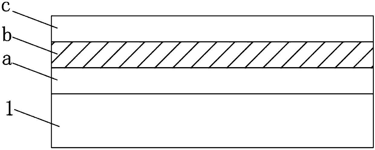
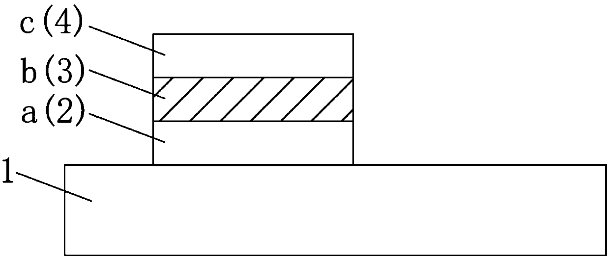
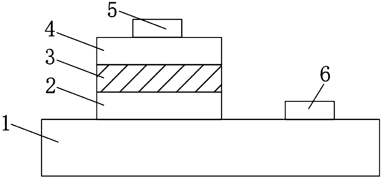
[0029] Step S1, on an N-type substrate 1 (preferably an N-type InAs substrate with a doping concentration of 1×10 19 cm -3 ) to form a detector mesa, the detector mesa includes an N-type InAsP / InAsSb superlattice absorption layer 2, an InPSb barrier layer 3 and an N-type InAsP / InAsSb stacked on the N-type substrate 1 in sequence Superlattice contact layer 4 .

[0030] Specifically, such as figure 1 As shown, in this step, after the N-type substrate 1 is subjected to high-temperature treatment to remove surface impurities, the stacked first N-type InAsP / InAsSb superlattice layer a, InPSb layer b, second N-type InAsP / InAsSb superlattice layer c. Among them, the growth source is TMIn, TMSb, AsH 3 and PH 3 , N-type dopant source is SiH 4 , the growth temperature is 600°C, and the reaction chamber pressure is 200Torr. Wherein, the InPSb layer b is not doped, has...


PUM

PropertyMeasurementUnit
thicknessaaaaaaaaaa
thicknessaaaaaaaaaa

Abstract

The invention discloses a manufacturing method of an infrared detector. The manufacturing method comprises the following steps: forming a detector mesa on an N-type substrate, wherein the detector mesa comprises an N-type InAsP / InAsSb superlattice absorption layer, an InPSb barrier layer and an N-type InAsP / InAsSb superlattice contact layer, which are sequentially formed on the N-type substrate ina stacked manner; and forming a first electrode on the N-type InAsP / InAsSb superlattice contact layer of the detector mesa, and forming a second electrode corresponding to the detector mesa on the N-type substrate. The invention also discloses the infrared detector manufactured by the manufacturing method. According to the invention, the problem that a heterojunction structure is difficult to form in the manufacturing process of the infrared detector is solved.

Description

technical field [0001] The invention relates to the field of semiconductors, in particular to an infrared detector and a manufacturing method thereof. Background technique [0002] Infrared radiation detection is an important part of infrared technology, widely used in thermal imaging, satellite remote sensing, gas monitoring, optical communication, spectral analysis and other fields. Antimonide II superlattice infrared detectors are considered to be one of the most ideal choices for the preparation of third-generation infrared detectors because of their good uniformity, low Auger recombination rate, and large wavelength adjustment range. Compared with mercury cadmium telluride infrared detectors (HgCdTe), it has better uniformity, repeatability, lower cost, and better performance in long-wave and very long-wave bands; compared with quantum well infrared detectors (QWIP), its quantum efficiency is higher High, smaller dark current, simpler process. [0003] At present, ant...

Claims


Application Information

Patent Timeline
Patent Type & Authority Applications(China)
IPC IPC(8): H01L31/11H01L31/0304H01L31/18C23C14/16C23C14/30C23C16/30C23C16/44
CPCC23C14/16C23C14/30C23C16/30C23C16/44H01L31/03046H01L31/11H01L31/1844Y02P70/50
Inventor 赵宇吴启花黄勇熊敏
Owner SUZHOU INST OF NANO TECH & NANO BIONICS CHINESE ACEDEMY OF SCI
Why Eureka
Try Eureka