Diarylamine substituted spirobifluorene compound and application in OLED device

A technology of diarylamine and spirobifluorene, which is applied in the fields of organic chemistry and optoelectronic devices, and can solve problems such as performance differences

Active Publication Date: 2020-06-02
CHANGZHOU TRONLY NEW ELECTRONICS MATERIALS +1
View PDF2 Cites 2 Cited by
  • Summary
  • Abstract
  • Description
  • Claims
  • Application Information

AI Technical Summary

Problems solved by technology

In addition, for the collocation of OLED devices with different structures, the photoelectric functional materials used ha...

Method used


Image

  • Diarylamine substituted spirobifluorene compound and application in OLED device
  • Diarylamine substituted spirobifluorene compound and application in OLED device
  • Diarylamine substituted spirobifluorene compound and application in OLED device

Examples


Embodiment C1

[0064] (1) Example C1: Synthesis of 2-bromo-6-chloro-9,9'-spirobifluorene

[0065]

[0066] Fully dry the experimental device, add 35g of 2-bromo-1,1'-biphenyl (152mmol) and 400mL of dried tetrahydrofuran into a 1L four-necked flask under nitrogen, stir and dissolve, then cool down to below -78°C with liquid nitrogen , slowly add 61mL of 2.5M (152mmol) n-BuLi n-hexane solution dropwise; after the dropwise addition, stir at -78°C for 1h, then add 45g (152mmol) 2-bromo-6-chloro- 9-fluorenone was solid, after the addition was completed, it was kept at -78°C for 1h, and then stirred at room temperature for 12h. After the reaction was completed, 4M hydrochloric acid solution was added dropwise to quench the reaction, extracted with ethyl acetate, the organic phase was washed with saturated brine, and the solvent was spin-dried to obtain intermediate alcohol B1.

[0067] Without any purification, it was fed into a 1L dry three-neck flask, 160mL of acetic acid and 5g of 36% hydro...

Embodiment D1

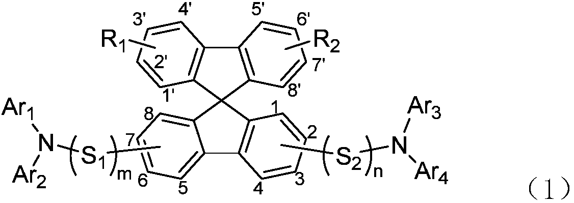
[0079] (1) Example D1: Synthesis of N-([1,1'-biphenyl-4-yl)-6-chloro-N-(9-9-dimethyl-9-fluoren-2-yl)- 9,9'-spirobifluorenyl-2-amine]

[0080]

[0081] The experimental device was fully dried, and 19.3 g (45 mmol) of 2-bromo-6-chloro-9,9'-spirobifluorene and 17.9 g (49.5 mmol) of N-[1,1 '-biphenyl-4-yl]-9,9-dimethyl-9H-fluorene-2-amine, then add dry and degassed toluene as solvent, add 6.5g (67.5mmol) sodium tert-butoxide, 1.2g (2.25mmol) catalyst 1,1'-bis(diphenylphosphino)ferrocene, heated to 100-105°C, reacted for 16h. After the reaction was completed, it was cooled to room temperature, diluted with toluene, filtered through a pad of silica gel, and the filtrate was evaporated to remove the solvent in vacuo to obtain a crude product, which was purified by column chromatography to obtain 18.6 g of product D1 with a yield of 58%.

[0082] MS[M+H] + =710.23.

[0083] (2)D2-D10

[0084] Referring to the preparation method of intermediate D1, intermediates D2-D10 were syn...

Embodiment 1

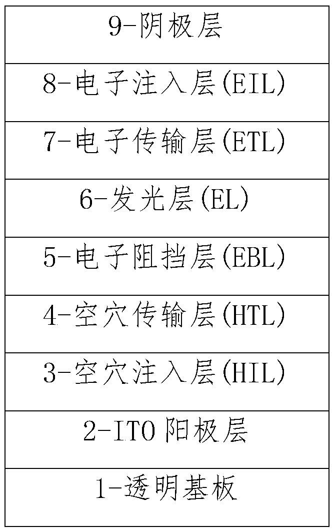
[0118] refer to figure 1 The structure shown is to manufacture an OLED device. The specific steps are: the glass substrate (Corning glass 50mm*50mm*0.7mm) coated with ITO (indium tin oxide) with a thickness of 130nm is ultrasonically washed for 5 minutes with isopropanol and pure water respectively, Then use ultraviolet ozone to clean, and then the glass substrate is transferred to the vacuum deposition chamber; the hole injection material HAT-CN is vacuumed with a thickness of 5 nm (about 10 -7 Torr) is thermally deposited on the transparent ITO electrode, thereby forming a hole injection layer; on the hole injection layer, the compound 1-192 synthesized in the above-mentioned preparation example with a thickness of 110nm is vacuum-deposited to form a hole transport layer; HT2 is vacuum-deposited with a thickness of 20nm on the transport layer to form an electron blocking layer; as a light-emitting layer, the vacuum-deposited host EB and 4% guest dopant BD have a thickness of...


PUM

PropertyMeasurementUnit
Thicknessaaaaaaaaaa
Thicknessaaaaaaaaaa

Abstract

The invention discloses an organic compound containing a diarylamine substituted spirobifluorene structure, wherein the organic compound has a structure represented by a chemical formula (1). The compound has high glass transition temperature, appropriate HOMO and LUMO energy levels, high Eg (energy gap) and high thermal stability, can sublimate under the conditions of no decomposition and no residue, has a good application effect in OLED devices, and can effectively improve the light emitting performance of the devices and prolong the service life of the devices.

Description

technical field [0001] The invention belongs to the technical field of organic chemistry and photoelectric devices, and in particular relates to a compound containing a diarylamine-substituted spirobifluorene (9,9'-Spirobifluorene) structure and its application in OLED devices. Background technique [0002] Compared with traditional liquid crystal display (LCD) panels, organic electroluminescent (OLED) devices have the advantages of self-illumination, high contrast, light and thin, good color saturation, wide viewing angle and fast response speed, etc., and are called "third-generation displays". ". With the wide application of OLED screens in smartphones, TVs, and automotive electronics markets, OLED panel shipments have shown a rapid growth trend, while LCD panel shipments have begun to decline, causing many manufacturers mainly engaged in LCD panel production to stop production or even go bankrupt. According to the latest data from HISMarkit, as the smartphone market has...

Claims


Application Information

Patent Timeline
IPC IPC(8): C07C211/61C07D209/88C07D219/02C07D307/91H01L51/54
CPCC07C211/61C07D307/91C07D209/88C07D219/02H10K85/624H10K85/636H10K85/633H10K85/6574H10K85/6572C07D213/16C07D239/26C07D405/10C07D405/14C07D403/04C07D409/04H10K99/00C07C211/54C07C209/74C07C2603/18H10K85/615H10K50/16H10K50/17H10K50/11
Inventor 钱晓春蒋建兴马培培孙杰
Owner CHANGZHOU TRONLY NEW ELECTRONICS MATERIALS
Why Eureka
Try Eureka