Window with infrared transparent conductive function

A technology of transparent conduction and transparent conduction layer, which is applied in the direction of equipment for manufacturing conduction/semiconduction layer, conduction layer on insulating carrier, circuit, etc. It can solve the problem that windows cannot take into account electromagnetic shielding and high infrared transmittance performance, etc. problems, achieve good infrared transmission and electromagnetic shielding performance, improve infrared transmittance, and high hardness

Active Publication Date: 2020-06-12
HARBIN INST OF TECH
View PDF7 Cites 5 Cited by
  • Summary
  • Abstract
  • Description
  • Claims
  • Application Information

AI Technical Summary

Problems solved by technology

[0007] The present invention aims to solve the technical problem that the existing windows with infrared transparent and conductive functions cannot take into account the performance of electromagnetic shielding and high infrared transmittance, and provides a window with infrared transparent and conductive functions

Method used


Image

  • Window with infrared transparent conductive function
  • Window with infrared transparent conductive function
  • Window with infrared transparent conductive function

Examples


specific Embodiment approach 1

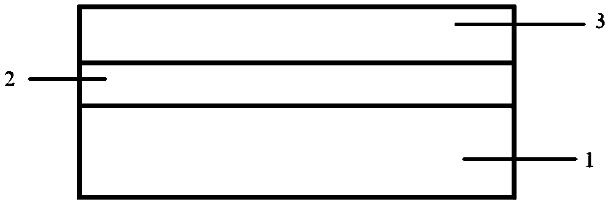
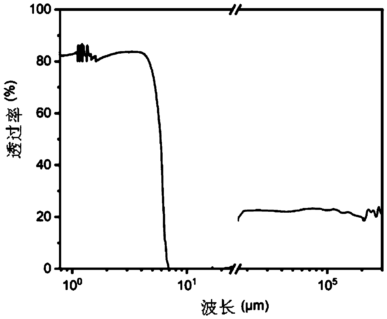
[0036] Embodiment 1: This embodiment is a window with an infrared transparent conductive function, which is specifically composed of a substrate, a transparent conductive layer and an infrared anti-reflection layer grown on the substrate in sequence;

[0037] The substrate is a sapphire substrate, the orientation is the (0001) crystal plane, the sapphire substrate is polished on both sides, and the thickness is 100 μm to 30000 μm;

[0038] The transparent conductive layer is made of tin-doped indium oxide (ITO), aluminum-doped zinc oxide (AZO), gallium-doped zinc oxide (GZO), fluorine-doped tin oxide (FTO), tin oxide (SnOx), Yttrium oxide doped ruthenium (YRO), nitrogen doped indium oxide (InNO) and indium oxide (In 2 o 3 ) in one or more laminates; the total thickness of the transparent conductive layer is 0.1 μm to 100 μm, and the average electron concentration is not higher than 1×10 20 cm -3 ;

[0039] The infrared antireflection layer is magnesium fluoride (MgF 2 ), ...

specific Embodiment approach 2

[0040] Embodiment 2: This embodiment is different from Embodiment 1 in that: the thickness of the substrate is 1 mm. Others are the same as the first embodiment.

specific Embodiment approach 3

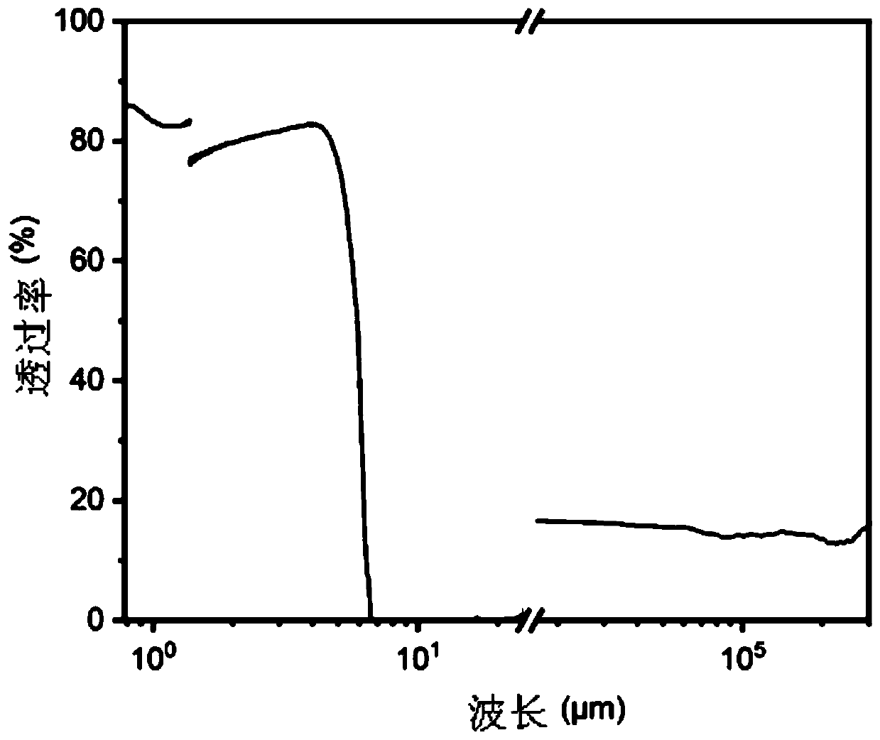
[0041] Embodiment 3: The difference between this embodiment and Embodiment 1 or 2 is that the total thickness of the transparent conductive layer is 0.89 μm, and the average electron concentration is 9.76×10 18 cm -3 . Others are the same as those in Embodiment 1 or 2.


PUM

PropertyMeasurementUnit
thicknessaaaaaaaaaa
thicknessaaaaaaaaaa
thicknessaaaaaaaaaa

Abstract

The invention discloses a window with an infrared transparent conductive function, and belongs to the field of infrared optical materials and the field of electronic materials. The invention aims to solve the technical problem that an existing window with an infrared transparent conductive function cannot give consideration to electromagnetic shielding and high infrared transmittance. The window with the infrared transparent conductive function is composed of a substrate, a transparent conductive layer and an infrared anti-reflection layer, wherein the transparent conductive layer and the infrared anti-reflection layer sequentially grow on the substrate. The transmittance of the window with the infrared transparent conductive function is not lower than 80% within the wavelength range of 0.78 mu m to 2.5 mu m; the transmittance is not lower than 75% within the wavelength range of 2.5-5 microns, the square resistance is not larger than 100 ohm/sq, and the shielding efficiency for 1GHz-18GHz electromagnetic waves is larger than 10dB. The preparation method is applied to preparation of the window with the infrared transparent conductive function.

Description

technical field [0001] The invention belongs to the fields of infrared optical materials and electronic materials. Background technique [0002] The infrared photoelectric system is the core component of the search, discovery and tracking multi-target functions in the process of weaponry, artificial intelligence and industrial automation, such as infrared search and tracking system or precise detection system, which has an irreplaceable role. However, in the actual use of complex electromagnetic interference environment, the infrared photoelectric system is urgently required to have the ability to resist external electromagnetic wave interference. At present, the widely used method is to fabricate noble metal grids such as Au on the surface of the hood of the infrared photoelectric system, and optimize the line width and period to achieve the purpose of not only transmitting infrared light but also effectively shielding electromagnetic waves. However, the processing of nobl...

Claims


Application Information

Patent Timeline
Patent Type & Authority Applications(China)
IPC IPC(8): H01B1/08H01B5/14H01B13/00C23C14/06C23C14/30C23C14/35
CPCC23C14/0694C23C14/30C23C14/352H01B1/08H01B5/14H01B13/0026
Inventor 杨磊徐梁格代兵郭帅杨振怀耿方娟高岗孙春强朱嘉琦
Owner HARBIN INST OF TECH
Why Eureka
Try Eureka