Preparation method of GaN-based planar Schottky varactor

A technology of varactors and base planes, which is applied in semiconductor/solid-state device manufacturing, electrical components, circuits, etc., can solve problems such as inability to meet high power requirements, achieve the effects of reducing parasitic capacitance, reducing errors, and improving surface quality

Active Publication Date: 2020-08-28
NAT SPACE SCI CENT CAS
View PDF15 Cites 1 Cited by
  • Summary
  • Abstract
  • Description
  • Claims
  • Application Information

AI Technical Summary

Problems solved by technology

[0003] At present, the core device of the solid-state frequency multiplier oscillation circuit is gallium arsenide (GaAs)-based Schottky diode. Due to the limitation of the domestic compound sem...

Method used


Image

  • Preparation method of GaN-based planar Schottky varactor
  • Preparation method of GaN-based planar Schottky varactor
  • Preparation method of GaN-based planar Schottky varactor

Examples


Embodiment 1

[0036] A preparation method of a GaN-based planar Schottky varactor, the preparation method comprising the steps of:

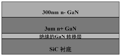
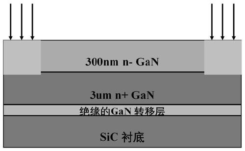
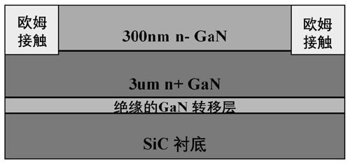
[0037] 1) GaN epitaxial wafers with a diameter of 2 inches of silicon carbide (SiC) substrates (which can improve the crystallization quality of GaN epitaxial layer materials and reduce dislocation density), such as figure 1 As shown, the epitaxial wafer structure from bottom to top is: 360um thick SiC substrate, insulating GaN transition layer, n-type heavily doped GaN layer with a thickness of 3um, and a doping concentration of 1*10 19 / cm -3 , an n-type lightly doped GaN layer with a thickness of 300nm, and a doping concentration of 2*10 17 / cm -3 ;

[0038] 2) Positioning calibration - production of alignment marks:

[0039] The lithography equipment uses a contact or stepper exposure machine to design an alignment pattern, and uses electron beam evaporation Ti / Au to complete the transfer of the alignment mark shown in the pattern on the epitaxial waf...


PUM


Abstract

The invention belongs to the field of manufacturing of semiconductor devices, and particularly relates to a preparation method of a GaN-based planar Schottky varactor. The preparation method comprisesthe steps of 1) manufacturing an alignment mark; 2) manufacturing an ohmic electrode; 3) manufacturing a Schottky metal eave structure through primary planarization; 4) conducting Schottky metal evaporation; 5) etching an insulating table; 6) carrying out secondary planarization; and 7) electroplating to form an air bridge, an electrode pad and interconnection metal to obtain the GaN-based planarSchottky varactor. The etching condition of the metal eave structure is effectively improved, the surface quality of the side wall is improved, and trapped charges on the surface of the side wall arereduced, so that the reverse bias characteristic of the device is improved; and errors introduced by the process of the air bridge structure are improved, and parasitic capacitance of the device is effectively reduced.

Description

technical field [0001] The invention belongs to the field of manufacturing semiconductor devices, in particular to a method for preparing a GaN-based planar Schottky varactor based on planarization technology. Background technique [0002] Terahertz wave is an electromagnetic wave between microwave and millimeter wave and infrared light. Its frequency range is usually between 100 GHz and 10 THz, and the corresponding wavelength is 0.03 to 3 mm. Since the 1990s, with the development of laser technology and compound semiconductor technology, people's research on terahertz science has made great progress. The terahertz frequency domain is in the transition zone from the macroscopic classical theory to the microscopic quantum theory. Due to its special spectral position, the terahertz wave exhibits many excellent characteristics, including: it can penetrate most non-metallic materials, and will not cause material Molecular ionization is especially suitable for biological tissue...

Claims


Application Information

Patent Timeline
IPC IPC(8): H01L29/93H01L29/872H01L21/329
CPCH01L29/93H01L29/872H01L29/66143Y02P70/50
Inventor 祁路伟张德海孟进
Owner NAT SPACE SCI CENT CAS
Why Eureka
Try Eureka