Method for realizing electron local passivation contact, and crystalline silicon solar cell and preparation method thereof

A crystalline silicon, partial technology, applied in the field of solar cell preparation, can solve the problems of difficulty in the application of partial passivation contact structures, cumbersome preparation steps, cumbersome process steps, etc., and achieve good industrialization potential, simple process, and good optical properties.

Active Publication Date: 2020-09-04
CHANGZHOU SHICHUANG ENERGY CO LTD
View PDF5 Cites 13 Cited by
  • Summary
  • Abstract
  • Description
  • Claims
  • Application Information

AI Technical Summary

Problems solved by technology

Photolithography belongs to the manufacturing method of semiconductor chips, the cost is high and the preparation steps are cumbersome; and the use of chemical slurry etching to prepare local contact passivation structures also requires doping on the polysilicon layer, preparing masks, printing protective or Etching-type chemical slurry, chemical etching, and mask removal, etc., the preparation steps are cumbe

Method used


Image

  • Method for realizing electron local passivation contact, and crystalline silicon solar cell and preparation method thereof
  • Method for realizing electron local passivation contact, and crystalline silicon solar cell and preparation method thereof
  • Method for realizing electron local passivation contact, and crystalline silicon solar cell and preparation method thereof

Examples


Embodiment 1

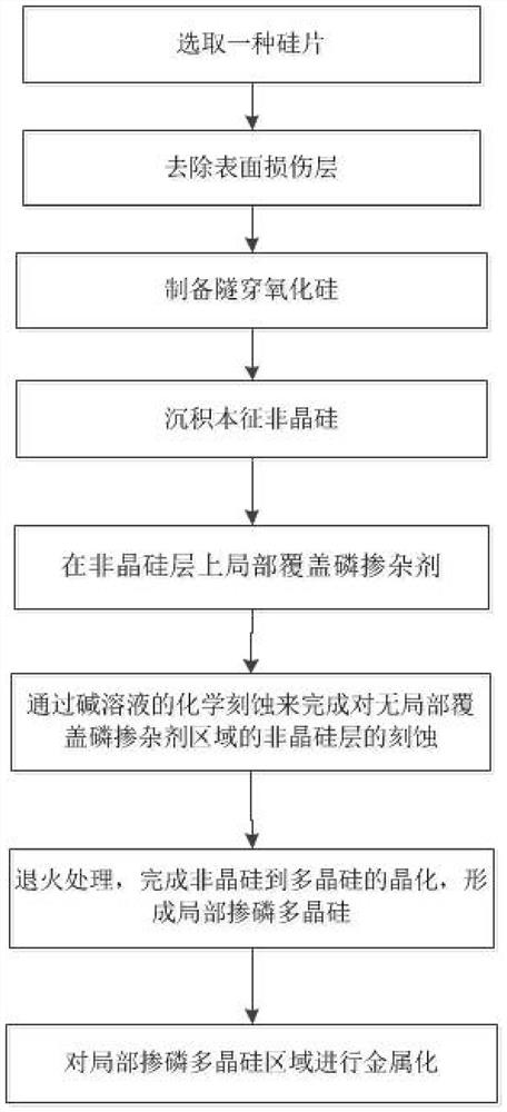
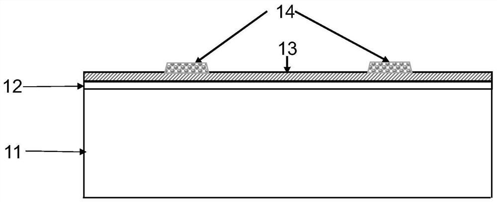
[0019] First of all, the present invention provides a method that can realize the electronic local passivation contact structure, which is combined with Embodiment 1 below figure 1 and Fig. 2, provide its main preparation process, but the following examples are only used to more clearly illustrate the technical solutions of the present invention, but not to limit the protection scope of the present invention. Embodiment 1 mainly comprises the following steps:

[0020] 1) A single crystal n-type silicon wafer or p-type silicon wafer is selected, and polycrystalline or quasi-monocrystalline silicon wafers can also be selected, but are not limited thereto. The selected silicon wafer is polished and etched with an alkaline solution (such as sodium hydroxide NaOH or potassium hydroxide KOH) or an acid solution (such as a mixed solution of nitric acid and hydrofluoric acid, etc.) to remove the damaged layer. Optionally, after removing the damaged layer, the alkali solution can be u...

Embodiment 3

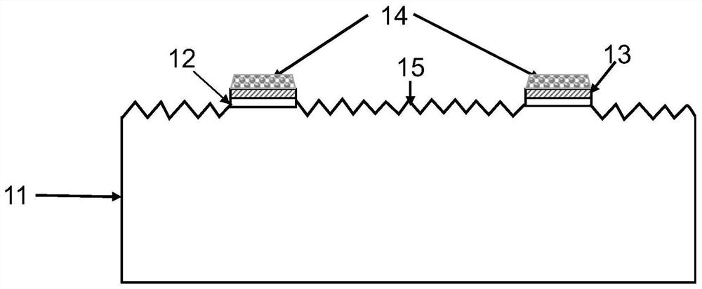
[0069] Embodiment 3 discloses a solar cell structure with an electronic local passivation contact structure and a preparation method thereof. The battery structure given in this embodiment is as follows image 3 As shown in , the front side of the cell uses a local passivation contact for electrons, and the back side of the cell uses a full-area hole passivation contact. The substrate material here is p-type single crystal silicon (or n-type single crystal silicon). The battery preparation method is as follows:

[0070] A1: Choose a 156mm*156mm (100) p-type monocrystalline silicon wafer with a resistivity of 1 Ω·cm and a thickness of 180 μm.

[0071] A2: NaOH solution is used to polish and remove the damaged layer (about 10 μm) on the surface of the p-type silicon wafer.

[0072] A3: Prepare a tunneling silicon oxide layer on the surface of the p-type silicon wafer by a thermal oxidation process, with a thickness of 1.5 nm and a refractive index of 1.46. The tunneling sili...

Embodiment 4

[0083] Embodiment 4 discloses another solar cell structure with electronic local passivation contact structure and its preparation method. The battery structure given in this embodiment is as follows Figure 4 As shown, the front side of the battery uses electronic local passivation contacts, and the back side of the battery uses p-type doped junctions and corresponding passivation films. In this example, the substrate material is n-type monocrystalline silicon (p-type monocrystalline silicon can also be used), and the battery preparation method is as follows:

[0084] B1: Select a 156mm*156mm (100) n-type monocrystalline silicon wafer with a resistivity of 1 Ω·cm and a thickness of 180 μm.

[0085] B2: Polishing with NaOH solution to remove the damaged layer (about 10 μm) on the surface of the n-type silicon wafer.

[0086] B3: Perform uniform boron doping on the entire surface of the n-type silicon wafer by ion implantation combined with furnace tube annealing, and the bor...


PUM

PropertyMeasurementUnit
Sheet resistanceaaaaaaaaaa
Thicknessaaaaaaaaaa
Thicknessaaaaaaaaaa

Abstract

The invention discloses a method for realizing electron local passivation contact. The method comprises the following steps: firstly, preparing a tunneling silicon oxide layer and an amorphous siliconlayer on a crystalline silicon substrate of which a damage layer is removed; then locally covering the amorphous silicon thin film with a phosphorus doping agent; etching off an amorphous silicon thin film layer which does not partially cover a phosphorus dopant region through an alkaline solution, fully crystallizing amorphous silicon into polycrystalline silicon through annealing, activating aphosphorus dopant and finishing redistribution of the phosphorus dopant in the polycrystalline silicon thin film, and finally preparing a metallized layer on the partially phosphorus-doped polycrystalline silicon thin film. Furthermore, the invention also discloses a crystalline silicon solar cell with the electron local passivation contact structure and a corresponding cell preparation method. The method disclosed by the invention is simple in process and relatively low in cost, and has good industrial potential; and the cell provided by the invention is good in front optical performance andlow in metallization recombination, and can obtain higher photon-generated carrier collection probability and less photon-generated carrier transmission loss.

Description

technical field [0001] The invention belongs to the technical field of solar cell preparation, and specifically relates to a method for realizing an electronic local passivation contact structure, and applying the electronic local passivation contact structure to a crystalline silicon solar cell and a corresponding cell preparation method. Background technique [0002] Passivated contact (Tunnel Oxide and Passivated Contact, TOPCon) solar cell is a new type of high-efficiency solar cell, which passivates crystalline silicon solar cells (hereinafter referred to as solar cells or cells) by tunneling silicon oxide and doped polycrystalline silicon. surface, to realize the selective passage of photogenerated carriers, that is, the majority carriers can enter the doped polysilicon film through the tunneling silicon oxide layer without hindrance and then be collected, while the minority carriers are in the tunnel The recombination rate at the interface of the silicon oxide and sil...

Claims


Application Information

Patent Timeline
IPC IPC(8): H01L31/18H01L31/0224H01L31/0216H01L31/068
CPCH01L31/02168H01L31/022425H01L31/068H01L31/1804H01L31/1864H01L31/1868Y02E10/546Y02E10/547Y02P70/50
Inventor 黄海冰张梦葛张胜军沈梦超绪欣吴智涵
Owner CHANGZHOU SHICHUANG ENERGY CO LTD
Why Eureka
Try Eureka