Gallium arsenide-doped single crystal growth process

A gallium arsenide single crystal and crystal growth technology, which is applied in the direction of single crystal growth, crystal growth, single crystal growth, etc., can solve the problems of B entry and B pollution, and achieve the improvement of single crystal rate, low oxygen content, and oxygen content low effect

Active Publication Date: 2020-11-06
SHANXI CHINA CRYSTAL TECH CO LTD
View PDF14 Cites 6 Cited by
  • Summary
  • Abstract
  • Description
  • Claims
  • Application Information

AI Technical Summary

Problems solved by technology

[0004] If silicon is doped in the process of VGF single crystal growth, since boron oxide is needed in the single crystal growth process, the presence of boron oxide Cause a large amount of B to enter the melt, resulting in B contamination

Method used


Image

  • Gallium arsenide-doped single crystal growth process
  • Gallium arsenide-doped single crystal growth process

Examples


Embodiment 1

[0043] S1. Polycrystalline synthesis

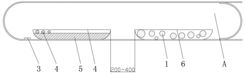
[0044](1) Loading: put high-purity arsenic and high-purity gallium into the clean first PBN boat and second PBN boat according to the ratio of (1.15~1.1):1 according to the operating procedures; put the silicon to be doped into Insert the end of the PBN boat filled with gallium; confirm that the distance between the first PBN boat and the second PBN boat is 200~400mm. In the vacant position of the quartz tube, place 5~100g of one or more of C, Ti, and Al as shown in Figure 1; in the figure: A is a polycrystalline quartz tube, 1 is arsenic particles, 2 is gallium liquid, and 3 is One or more of C, Ti, Al, 4 is a silicon particle, 5 is a first PBN boat, 6 is a second PBN boat; the silicon particle rests on the surface of the gallium liquid.

[0045] (2) Baking material: place the loaded quartz tube on the oven, adjust the cap, tighten the clamp, cover the oven cover and turn on the vacuum pump to vacuum the vacuum (1~9*10 -4 )~(1~9*10 -2...

Embodiment 2

[0057] S1. Polycrystalline synthesis

[0058] (1) Loading: put high-purity arsenic and high-purity gallium into the clean first PBN boat and the second PBN boat according to the ratio of (1.15~1.1):1 according to the operating procedures; confirm the first PBN boat The distance from the second PBN boat is 200~400mm. In the vacant position of the quartz tube, such as figure 1 Place 5~100g of one or more of C, Ti, Al as shown.

[0059] (2) Baking material: place the loaded quartz tube on the oven, adjust the cap, tighten the clamp, cover the oven cover and turn on the vacuum pump to vacuum the vacuum (1~9*10 -4 )~(1~9*10 -2 ) Pa, bake for 2~4h.

[0060] (3) Welded pipe: Turn off the power of the oven to cool down, open the furnace cover, wrap the quartz tube with wet heat insulation cotton, put on gloves, first turn on the hydrogen to ignite, then turn on the oxygen to adjust the fire, and preheat on a low fire for more than 1 minute. Adjust the firepower to adjust the fire...


PUM


Abstract

The invention relates to the technical field of semiconductor material preparation, and in particular, relates to a gallium arsenide-doped single crystal growth process; oxygen released in the environment and in the high-temperature process of arsenic, gallium and a quartz tube is absorbed by adding materials with high oxygen reaction activity in two links of polycrystalline synthesis and single crystal growth, and oxygen pairs are preventd from entering polycrystals and single crystals, so the influence of oxygen pollution on the material performance is greatly reduced. Si doping is carried out in the polycrystalline synthesis process, silicon enters gallium arsenide and performs effective occupying, boron oxide does not exist, and polycrystalline synthesis does not cause B to pollute polycrystalline. C, Al or Ti is placed in a quartz tube to absorb oxygen in the quartz tube in the single crystal growth process, the oxygen content in the single crystal is controlled, and polycrystalline doped impurities are not added any more. During single crystal growth, boron oxide is added to improve the single crystal rate and realize selective adsorption of impurities. The desired crystal properties are achieved.

Description

technical field [0001] The invention relates to the technical field of semiconductor material preparation, and more specifically, to a doped gallium arsenide single crystal growth process. Background technique [0002] Gallium arsenide (GaAs) material is the most important material in the second generation of new compound semiconductors after silicon single crystal. It has excellent performance, high electron mobility and photoelectric conversion efficiency, and is widely used in the fields of microelectronics and optoelectronics. Single crystal substrates have been used in the manufacture of high-brightness LEDs, high-power LDs, microwave power devices, and monolithic circuits, and are widely used in luminescent displays, optical storage, mobile communications, national defense equipment, aerospace and other fields. In addition, GaAs-based solar cells have high conversion efficiency and good radiation resistance to become a new generation of high-performance, long-life spa...

Claims


Application Information

Patent Timeline
Patent Type & Authority Applications(China)
IPC IPC(8): C30B29/42C30B11/06
CPCC30B11/065C30B29/42
Inventor 高佑君柴晓磊樊海强
Owner SHANXI CHINA CRYSTAL TECH CO LTD
Why Eureka
Try Eureka