Double-sided PERC solar cell and preparation method thereof

A solar cell, double-sided technology, applied in circuits, photovoltaic power generation, electrical components, etc., can solve the problems of increased production process, surface damage of silicon wafers, increased fragmentation rate, etc., to avoid mechanical damage and fragmentation rate, and simplify the production process. , the effect of reducing production costs

Inactive Publication Date: 2020-12-25
CHANGZHOU SHICHUANG ENERGY CO LTD
View PDF7 Cites 1 Cited by
  • Summary
  • Abstract
  • Description
  • Claims
  • Application Information

AI Technical Summary

Problems solved by technology

Because the laser is used to open the passivation film on the back, it not only increases the production process, but also the laser energy is high, which is easy to cause damage to the surface of the silicon wafer, which leads to an increase in the fragmentation rate during the battery production process, and also affects the mechanical load performance of the component end.
In addition, since the back of the double-sided battery also has the function of generating electricity, the printing accuracy of the back electrode and the back grid line is high during production. At present, it is mainly solved by adding a high-precision camera to the original printing equipment, which increases the production cost.

Method used


Image

  • Double-sided PERC solar cell and preparation method thereof
  • Double-sided PERC solar cell and preparation method thereof

Examples


Embodiment 1

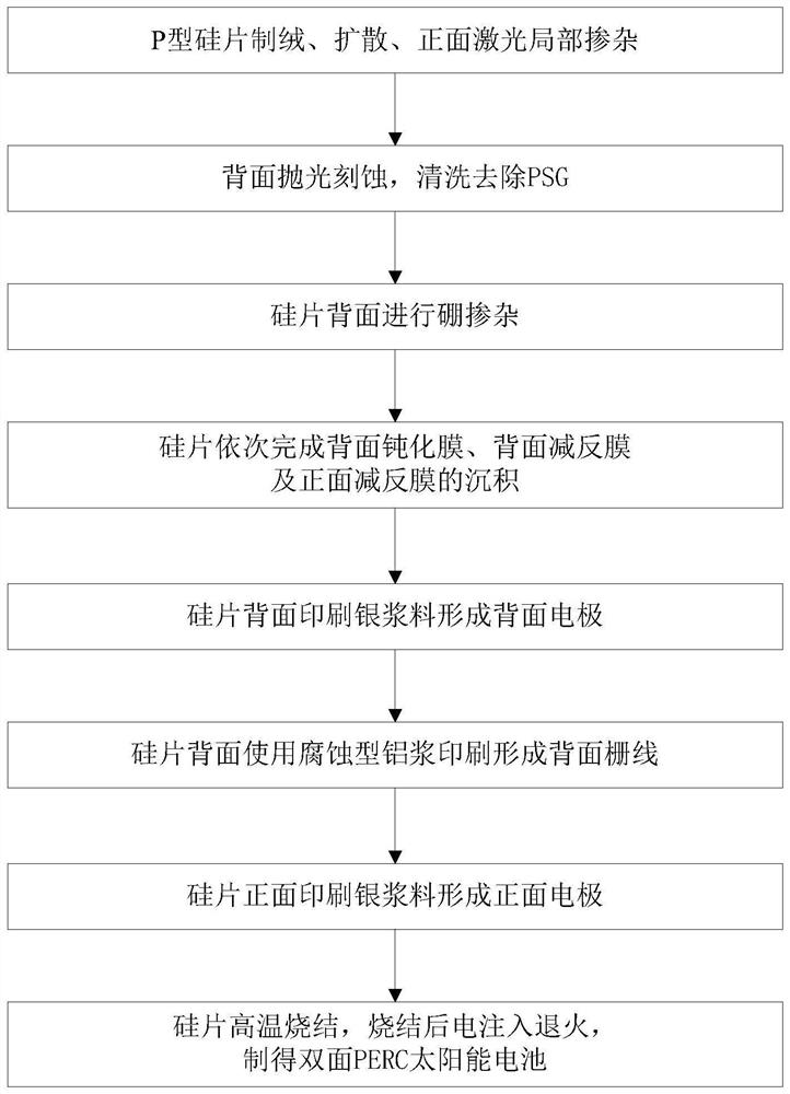
[0048] Such as figure 1 , the preparation method of a kind of double-sided PERC solar cell of the present embodiment, comprises the following steps:

[0049] (1) Take a P-type silicon wafer for texturing, diffuse the textured silicon wafer to form a PN junction on the front side, and then do laser doping on the front side to form a local heavily doped region N++;

[0050] (2) The silicon wafer is polished and etched on the back, the PN junction on the back and side is removed after diffusion, and the phosphosilicate glass PSG on the front is cleaned;

[0051] (3) Boron doping is performed on the back of the silicon wafer by ion implantation to form a doped region P+, where the boron doping concentration is 1×10 20 cm -3 ;

[0052] (4) Clean the silicon wafer, and complete the AlO on the back side in turn x Thin film, backside SiN x Thin film and front SiN x deposition of thin films in which AlO x The thickness of the film is 3nm;

[0053] (5) Print silver paste on the ba...

Embodiment 2

[0062] A kind of preparation method of double-sided PERC solar cell of the present embodiment, comprises the following steps:

[0063] (1) Take a P-type silicon wafer for texturing, diffuse the textured silicon wafer to form a PN junction on the front side, and then do laser doping on the front side to form a local heavily doped region N++;

[0064] (2) The silicon wafer is polished and etched on the back, the PN junction on the back and side is removed after diffusion, and the phosphosilicate glass PSG on the front is cleaned;

[0065] (3) Boron doping is carried out on the back of the silicon wafer by the amorphous silicon doping method to form a doped region P+, where the boron doping concentration is 8×10 19 cm -3 ;

[0066] (4) Clean the silicon wafer and complete the SiO on the back side in turn x Thin film, backside SiN x Thin film and front SiN x deposition of thin films in which SiO x The thickness of the film is 60nm;

[0067] (5) Print silver paste on the bac...

Embodiment 3

[0074] A kind of preparation method of double-sided PERC solar cell of the present embodiment, comprises the following steps:

[0075] (1) Take a P-type silicon wafer for texturing, diffuse the textured silicon wafer to form a PN junction on the front side, and then do laser doping on the front side to form a local heavily doped region N++;

[0076] (2) The silicon wafer is polished and etched on the back, the PN junction on the back and side is removed after diffusion, and the phosphosilicate glass PSG on the front is cleaned;

[0077] (3) Boron doping is performed on the back of the silicon wafer by high-temperature diffusion method to form a doped region P+, where the boron doping concentration is 5×10 18 cm -3 ;

[0078] (4) Clean the silicon wafer, and complete the AlO on the back side in turn x Thin film, backside SiN x Thin film and front SiN x deposition of thin films in which AlO x The thickness of the film is 5nm;

[0079] (5) Print silver paste on the back of...


PUM

PropertyMeasurementUnit
thicknessaaaaaaaaaa
thicknessaaaaaaaaaa

Abstract

The invention discloses a double-sided PERC solar cell and a preparation method thereof. The preparation method comprises the following steps of: performing texturing, diffusion, front laser doping, back polishing and etching, back passivation film deposition, back anti-reflection film deposition and front anti-reflection film deposition on a P-type silicon wafer; and printing a back electrode andback grid lines on the back anti-reflection film, printing a front electrode on the front anti-reflection film, and performing sintering and electric injection annealing. The back grid lines are printed by adopting corrosion type aluminum paste, and the corrosion type aluminum paste etches the back anti-reflection film and the back passivation film in the sintering process to form ohmic contact with the silicon wafer. According to the method, the corrosion type aluminum paste is printed on the back surface of the cell, the back anti-reflection film and the passivation film are etched and penetrated during sintering to realize local opening, an existing laser opening process is replaced, good ohmic contact between metal aluminum and a silicon wafer is realized in combination with back surface boron doping, and mechanical damage and fragment rate caused by laser opening are avoided; and the production process is simplified, and the production cost is reduced.

Description

technical field [0001] The invention relates to a PERC solar cell, in particular to a double-sided PERC solar cell and a preparation method. Background technique [0002] Passivated emitter back contact solar cells (PERC cells) are cells that have been mass-produced in recent years. Its mature back passivation technology is suitable for single crystal and polycrystalline silicon wafers, which can increase the conversion efficiency of crystalline silicon solar cells by more than 1%. . Passivated emitter back contact technology has gradually become a standard process for crystalline silicon solar cells. Its core technology is to cover the back of the silicon wafer with a thin film of aluminum oxide, silicon oxide or silicon oxynitride, which plays a role in passivating the surface of the silicon wafer. Improve the effect of long wave response. Double-sided PERC solar cells are newly developed high-efficiency solar cells that take into account both back passivation technology...

Claims


Application Information

Patent Timeline
Patent Type & Authority Applications(China)
IPC IPC(8): H01L31/18H01L31/0216H01L31/0224H01L31/068
CPCH01L31/02168H01L31/022425H01L31/068H01L31/1804H01L31/1864H01L31/1868Y02E10/547Y02P70/50
Inventor 孟祥熙许佳平
Owner CHANGZHOU SHICHUANG ENERGY CO LTD
Why Eureka
Try Eureka