Power semiconductor device with insulation structure in cell and preparation method
A technology for power semiconductors and power devices, which is applied in the field of power semiconductor devices with insulating structures in cells and their preparation, and can solve the problems of low reliability of strong fields and poor temperature tolerance.
- Summary
- Abstract
- Description
- Claims
- Application Information
AI Technical Summary
Problems solved by technology
Method used
Image

Examples
preparation example Construction
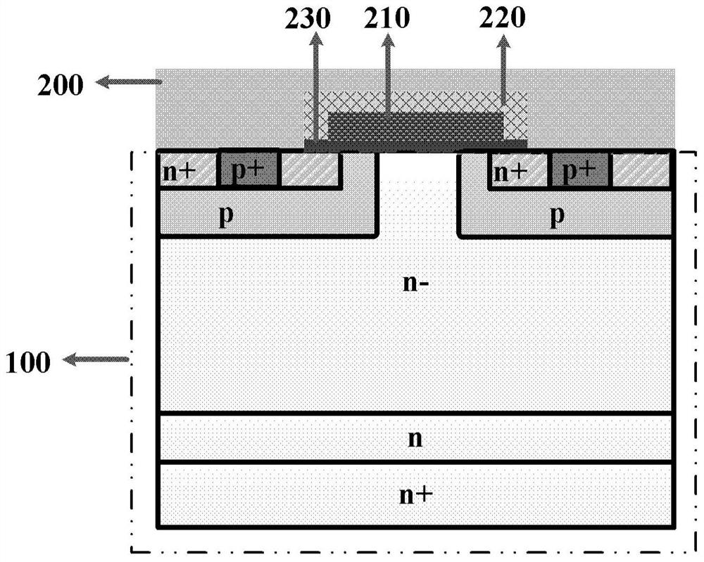
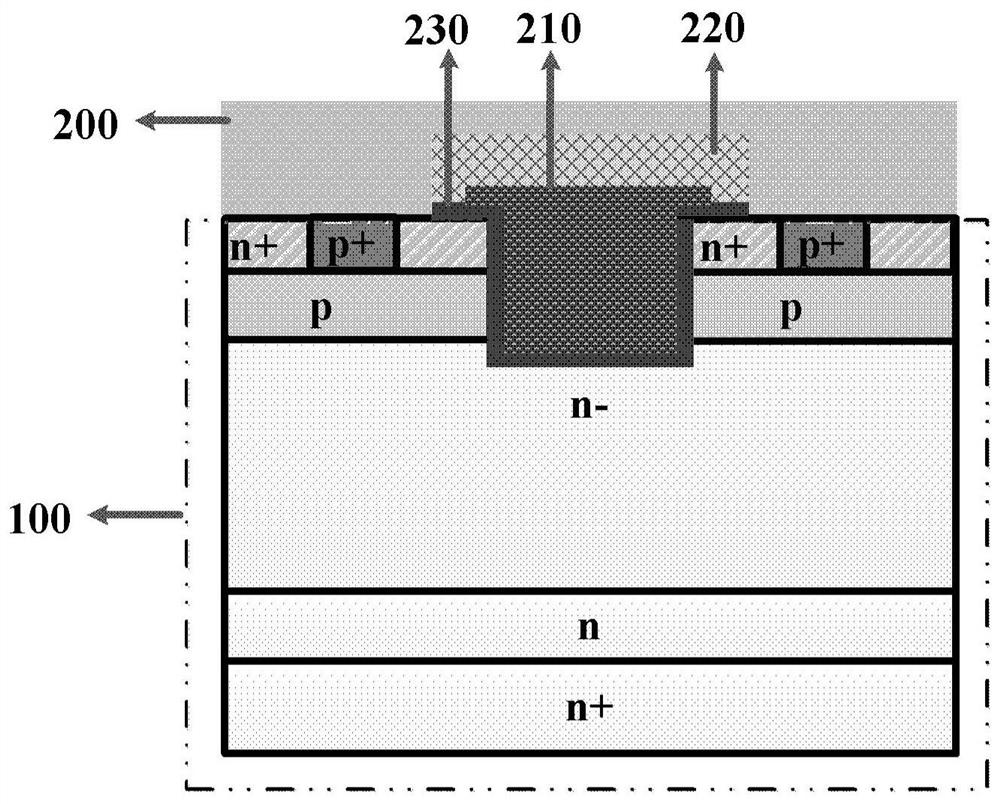
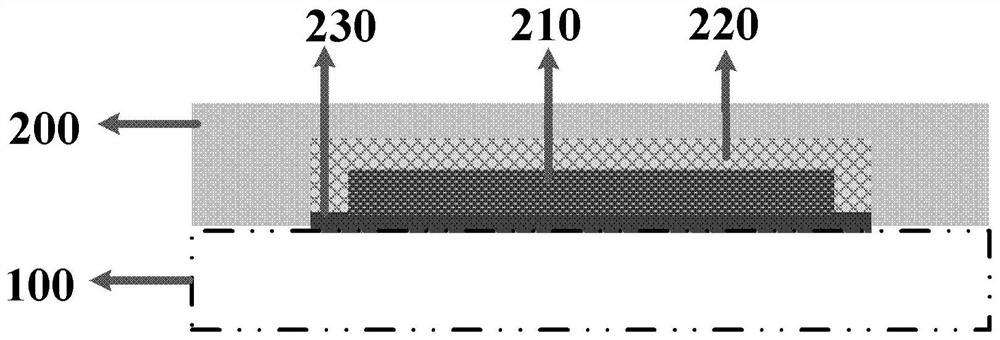
[0041] The second embodiment of the present disclosure provides a method for manufacturing a power semiconductor device with an insulating structure in a cell, please refer to Figure 4 , including: S1, cleaning the power device cell unit 100, forming a gate oxide layer 230 and a gate electrode contact 210 on the upper part of the cell unit 100; S2, autothermally oxidizing the surface of the gate electrode contact 210 to form a dense dielectric 300; Dielectric 300 first deposits high dielectric constant or high thermal conductivity and its combination thin film layer 310, and then deposits passivation dielectric thin film layer 320; Electrical constant or high thermal conductivity and its combination thin film layer 310 ; S4 , depositing source electrode contact 200 on the upper surface of power device unit cell 100 and composite interlayer 220 .
[0042] Cleaning the power device cell unit 100 in S1 is standard surface cleaning. The gate oxide layer 230 is made by thermal oxi...
Embodiment 1
[0054] structured as Figure 5 As shown, among them,
[0055] Step S1: cleaning the power device cell unit, first cleaning the surface of the power device cell unit 100, specifically:
[0056] a. Use acetone and ethanol to ultrasonically clean three times in sequence, and then rinse with deionized water.
[0057] b. Put the SiC epitaxial material substrate after organic ultrasonication into concentrated sulfuric acid and hydrogen peroxide solution and cook for at least 10 minutes.
[0058] c. Boil the SiC epitaxial material substrate boiled in concentrated sulfuric acid with No. 1 solution and No. 2 solution for 15 minutes, rinse with deionized water, and blow dry with nitrogen gas for use. The No. 1 liquid is a mixture of ammonia, hydrogen peroxide and deionized water, the volume ratio of ammonia: hydrogen peroxide: deionized water = 1: 2: 5, and the No. 2 liquid is a mixture of hydrochloric acid, hydrogen peroxide and deionized water. Mixed solution, hydrochloric acid: hy...
Embodiment 2
[0069] structured as Figure 6 As shown, among them,
[0070] Steps S1-S2, and S4 are the same as in Embodiment 1, the difference is,
[0071] Step S3: forming a composite inner insulating layer, the composite inner insulating layer includes a dielectric 300, a dielectric 310 and a dielectric 320 from bottom to top, and the specific steps include:
[0072] By physical, chemical and other etching methods, such as reactive ion etching (RIE) or inductively coupled plasma (ICP), etc., the gate electrode contact 210 is micro-etched, and the etching gas can be SF 6 / O 2 、NF 3 / Ar, CF 4 、H 2 / SiH 4 , HBr, CHF 3 / O 2 、C 4 f 8 / O 2 、BCl 3 / Cl 2 gas or combination to form an arcuate structure, using a low-temperature oxidation process (900°C) to autothermally oxidize the surface of the polysilicon gate electrode contact 210 to form a dense dielectric 300, the thickness of the dielectric 300 is 1-100nm, and pass through 1000 -1200°C annealing process for passivation.
[00...
PUM
| Property | Measurement | Unit |
|---|---|---|
| thickness | aaaaa | aaaaa |
| thickness | aaaaa | aaaaa |
Abstract
Description
Claims
Application Information
 - R&D Engineer
- R&D Manager
- IP Professional
- Industry Leading Data Capabilities
- Powerful AI technology
- Patent DNA Extraction
Browse by: Latest US Patents, China's latest patents, Technical Efficacy Thesaurus, Application Domain, Technology Topic.
© 2024 PatSnap. All rights reserved.Legal|Privacy policy|Modern Slavery Act Transparency Statement|Sitemap