Photoelectric detector employing gate modulation graphene/semiconductor Schottky junction and preparation method

A photodetector and semiconductor technology, applied in the field of photodetectors, can solve the problems of long response time, easy generation of dark current, carrier collection efficiency, low migration rate, etc., so as to reduce dark current and increase photocurrent. and responsiveness effects

Pending Publication Date: 2021-04-09
SOUTH CHINA UNIV OF TECH
View PDF0 Cites 2 Cited by
  • Summary
  • Abstract
  • Description
  • Claims
  • Application Information

AI Technical Summary

Problems solved by technology

[0003] The traditional MSM Schottky junction detector relies on biasing both ends of the device to form a built-in electric field for collecting carriers, but the field strength of the Schottky barrier and the applied bias electric field is not as good as that of PIN, APD and other devices The built-in electric field of the PN junction is strong (because under the same reverse bias voltage

Method used


Image

  • Photoelectric detector employing gate modulation graphene/semiconductor Schottky junction and preparation method
  • Photoelectric detector employing gate modulation graphene/semiconductor Schottky junction and preparation method
  • Photoelectric detector employing gate modulation graphene/semiconductor Schottky junction and preparation method

Examples


Embodiment 1

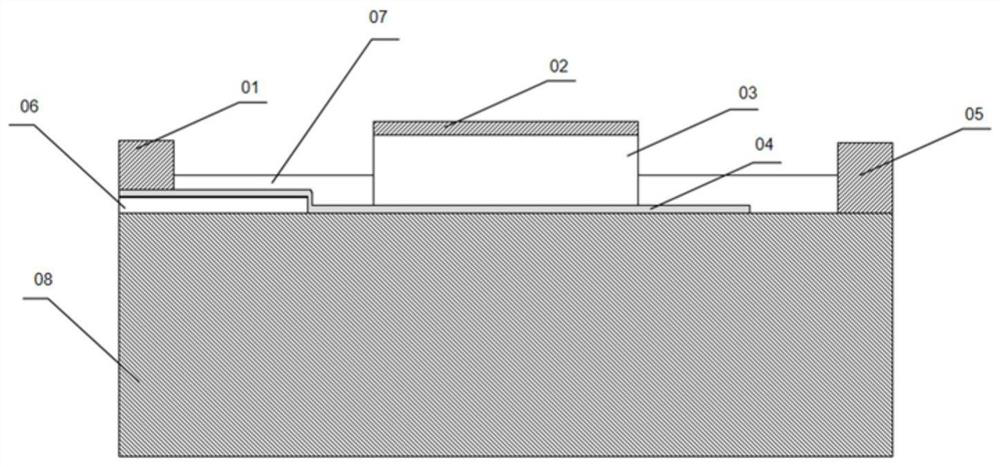
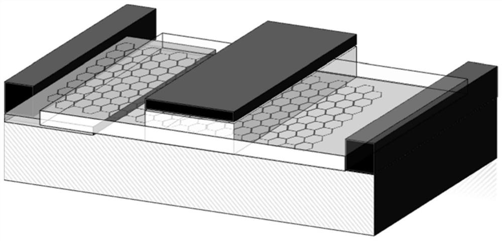
[0041] Such as figure 1 and figure 2 As shown, a photodetector adopting gate modulation graphene / semiconductor Schottky junction includes a substrate 08, a semiconductor layer is arranged on the substrate, and the insulating layer 06 is arranged on the semiconductor layer, and only covers the semiconductor layer A part of the area, the present embodiment 1 specifically covers the left part of the semiconductor layer, as an insulating layer that isolates a part of the graphene from contacting the semiconductor layer, and provides a platform for the graphene to contact the electrode, and its shape can change according to the requirements of the electrode. The graphene layer 04 is arranged on the insulating layer and part of the semiconductor layer, and the length ratio of the graphene on the insulating layer and on the semiconductor layer is 1:2-1:3; the transparent passivation layer 07 and the piezoelectric gate layer 03 is set on the graphene layer, the first metal electrode...

Embodiment 2

[0050] Such as Figure 3-Figure 7 Shown, the preparation method of above-mentioned embodiment 1 photodetector, comprises the steps:

[0051] (1) The substrate is high-resistance single-crystal silicon with (100) crystal orientation, and a high-quality germanium epitaxial layer with a thickness of 1 μm is grown on the high-resistance single-crystal silicon wafer, and the growth process adopts a two-step method of high temperature and low temperature. First, the received Si(100) substrate was annealed at 900 °C in air for 5 h before growth to obtain an atomically flat surface. Secondly, use ethanol deionized water to clean the substrate surface contamination, and put it into a vacuum of 2.0×10 -10 Torr's ultra-high vacuum MBE chamber. The growth of Ge adopts the solid-source MBE method. First, a ~20nm germanium buffer layer is grown on the Si(100) substrate at 500°C to suppress island growth; then the temperature is raised to 750°C, and the growth thickness is 980nm. Ge layer...


PUM

PropertyMeasurementUnit
Thicknessaaaaaaaaaa
Thicknessaaaaaaaaaa
Thicknessaaaaaaaaaa

Abstract

The invention discloses a photoelectric detector employing a gate modulation graphene/semiconductor Schottky junction and a preparation method. The photoelectric detector comprises a substrate, wherein the substrate is provided with a semiconductor layer, the semiconductor layer is provided with an insulating layer, the insulating layer and a part of the semiconductor layer are provided with a graphene layer, a transparent passivation layer and a piezoelectric gate layer are disposed on the graphene layer, a gate top electrode is arranged on the piezoelectric gate layer, a second metal electrode and the semiconductor layer form Schottky contact, and a first metal electrode and the graphene layer form ohmic contact. The photoelectric detector has the advantages that the structure is simple, the reliability is high, the influence of the manufacturing process on the core structure is small, the light response of the device can be regulated and controlled, and the photoelectric detector with high responsivity and low dark current is prepared.

Description

technical field [0001] The invention relates to the technical field of photodetectors, in particular to a photodetector using a grid-modulated graphene / semiconductor Schottky junction and a preparation method thereof. Background technique [0002] A photodetector is a device that converts optical signals into electrical signals for output. It is an indispensable key component in the fields of optical fiber communication, image sensors, visible light transmission, and optical chip interconnection and integration. Currently commonly used photodetectors are classified according to structure: PIN photodiode, avalanche diode (APD), metal-semiconductor-metal (MSM) diode, superlattice avalanche diode (SAPD), and waveguide photodetector (WPD). Cavity-enhanced photodetectors (RCEPD), etc., are classified according to the metal electrode and semiconductor contact types: ohmic contact and Schottky contact. Materials used include Si, Ge, GaAs, InP, GaP, GaN, In x Ga 1-x N, ZnO, MoS ...

Claims


Application Information

Patent Timeline
IPC IPC(8): H01L31/108H01L31/0224H01L31/028H01L31/18
CPCH01L31/022408H01L31/028H01L31/1085H01L31/18H01L31/1804Y02P70/50
Inventor 李国强陈胜王文樑柴吉星孔德麒
Owner SOUTH CHINA UNIV OF TECH
Why Eureka
Try Eureka