Composite substrate and manufacturing method thereof
A composite substrate and manufacturing method technology, applied in the direction of electrical components, circuits, semiconductor devices, etc., can solve problems such as slow progress, achieve the effects of improving crystal quality, improving refractive index difference, and increasing the probability of light emission
- Summary
- Abstract
- Description
- Claims
- Application Information
AI Technical Summary
Problems solved by technology
Method used
Image
Examples
Embodiment 1
[0037] Adopt above-mentioned scheme, specifically manufacture with the following steps:
[0038] 1. Put the sapphire substrate into the plasma-enhanced chemical vapor deposition equipment, control the process conditions, feed silane and carbon dioxide gas, and form a layer of SiO with a thickness of 100nm on the sapphire surface 2 mask;
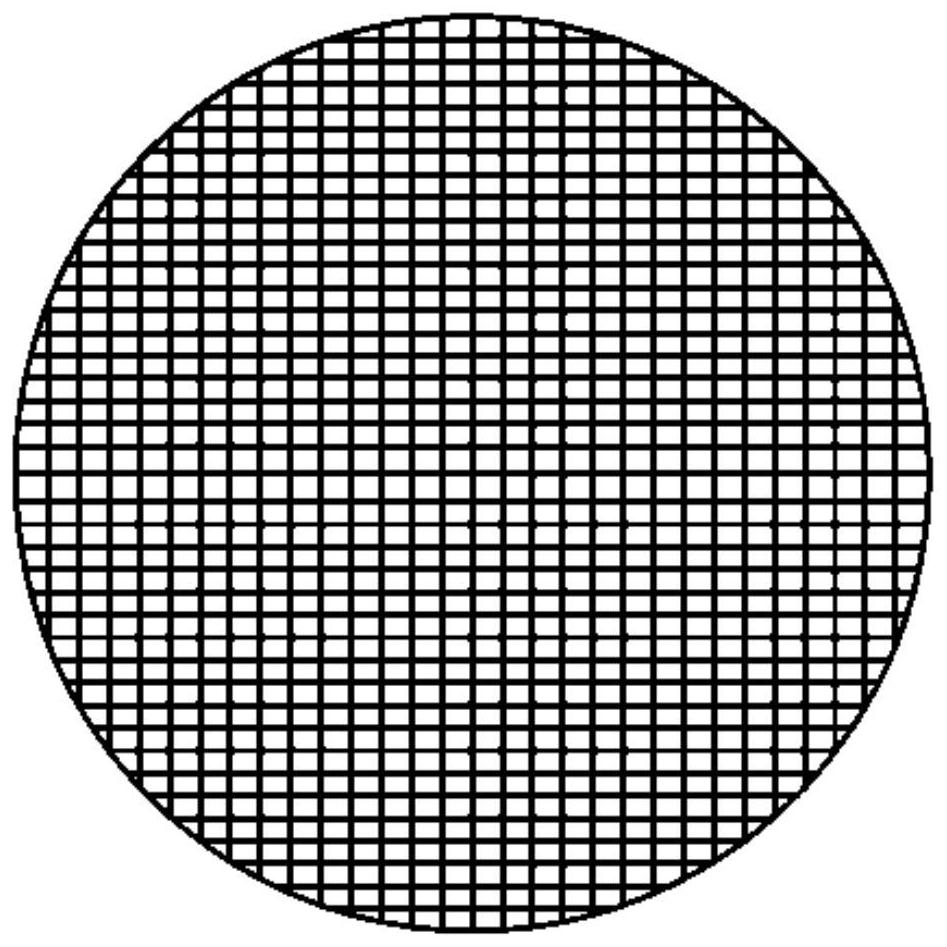
[0039] 2. will grow with SiO 2 The sapphire substrate of the mask is put into a laser cutting machine for cutting, and M vertically staggered grooves are formed on the surface. The groove width is 100 μm and the depth is 50 μm.
[0040] 3. Use a washing machine to clean the sapphire substrate to remove impurities in the groove.
[0041] 4. Put the cleaned substrate into the physical vapor deposition equipment, control the process conditions, and grow a layer of SiO with a thickness of 40 μm 2 The heterogeneous filling layer, and then control the process conditions to grow a magnesium fluoride filling layer with a thickness of 9.8 μm.
[...
Embodiment 2
[0045] Adopt above-mentioned scheme, specifically manufacture with the following steps:
[0046] 1. Put the sapphire substrate into the plasma-enhanced chemical vapor deposition equipment, control the process conditions, feed silane and carbon dioxide gas, and form a layer of SiO with a thickness of 100nm on the sapphire surface 2 mask;
[0047] 2. will grow with SiO 2 The sapphire substrate of the mask is put into a laser cutting machine for cutting, and M vertically staggered grooves are formed on the surface. The groove width is 100 μm and the depth is 50 μm.
[0048] 3. Use a washing machine to clean the sapphire substrate to remove impurities in the groove.
[0049] 4. Put the cleaned substrate into the physical vapor deposition equipment, control the process conditions, and grow a layer of SiO with a thickness of 40 μm 2 Heterogeneous filling layer, and then control the process conditions to grow a layer of magnesium fluoride (MgF 2 ) filling layer.
[0050] 5. Take ...
Embodiment 3
[0054] Adopt above-mentioned scheme, specifically manufacture with the following steps:
[0055] 1. Put the sapphire substrate into the plasma-enhanced chemical vapor deposition equipment, control the process conditions, feed silane and carbon dioxide gas, and form a layer of SiO with a thickness of 100nm on the sapphire surface 2 mask;
[0056] 2. will grow with SiO 2 The sapphire substrate of the mask is put into a laser cutting machine for cutting, and M vertically staggered grooves are formed on the surface. The groove width is 100 μm and the depth is 30 μm.
[0057] 3. Use a washing machine to clean the sapphire substrate to remove impurities in the groove.
[0058] 4. Put the cleaned substrate into the physical vapor deposition equipment, control the process conditions, first grow a zinc oxide (ZnO) heterogeneous filling layer with a thickness of 25 μm, and then control the process conditions to grow a layer with a thickness of 4.7 μm titanium dioxide (TiO 2 ) filli...
PUM
| Property | Measurement | Unit |
|---|---|---|
| Thickness | aaaaa | aaaaa |
| Width | aaaaa | aaaaa |
| Thickness | aaaaa | aaaaa |
Abstract
Description
Claims
Application Information
 - R&D Engineer
- R&D Manager
- IP Professional
- Industry Leading Data Capabilities
- Powerful AI technology
- Patent DNA Extraction
Browse by: Latest US Patents, China's latest patents, Technical Efficacy Thesaurus, Application Domain, Technology Topic, Popular Technical Reports.
© 2024 PatSnap. All rights reserved.Legal|Privacy policy|Modern Slavery Act Transparency Statement|Sitemap|About US| Contact US: help@patsnap.com


