Split gate trench power semiconductor device

A power semiconductor and split gate technology, which is applied to semiconductor devices, electrical components, circuits, etc., can solve the problems such as the imbalance of the compromise relationship between chip on-state loss and switching loss, the adverse effects of chip turn-on and turn-off, and the increase of chip switching loss. , to reduce parasitic effects, shorten the Miller platform, and improve reliability

Active Publication Date: 2021-05-11
ZHUZHOU CSR TIMES ELECTRIC CO LTD
View PDF4 Cites 0 Cited by
  • Summary
  • Abstract
  • Description
  • Claims
  • Application Information

AI Technical Summary

Problems solved by technology

However, as the trench gate density increases, it will lead to higher parasitic capacitance of the chip, which will have an adverse effect on the turn-on and turn-off of the chip, increase the switching loss of the chip, and lead to a compromise between the on-state loss and switching loss of the chip. out of balance
[0004] In addition, during the long-term use of power semiconductor devices, the oxide layer at the bottom of the trench is under high pressure for a long time, and the plasma in the body will repeatedly impact the oxide layer at the bottom of the trench during the chip switching process, affecting the reliability of the chip for long-term use

Method used


Image

  • Split gate trench power semiconductor device
  • Split gate trench power semiconductor device
  • Split gate trench power semiconductor device

Examples


no. 1 example

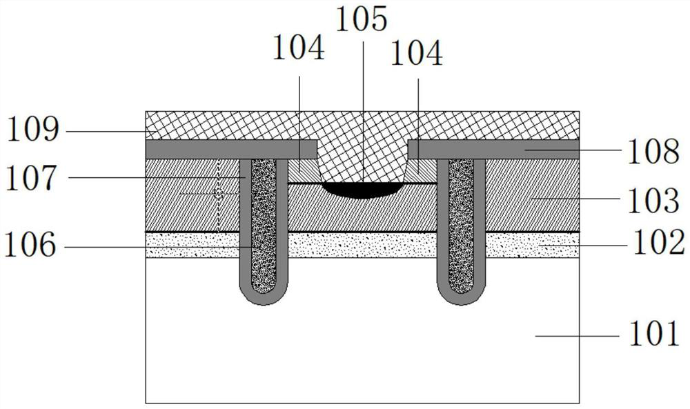
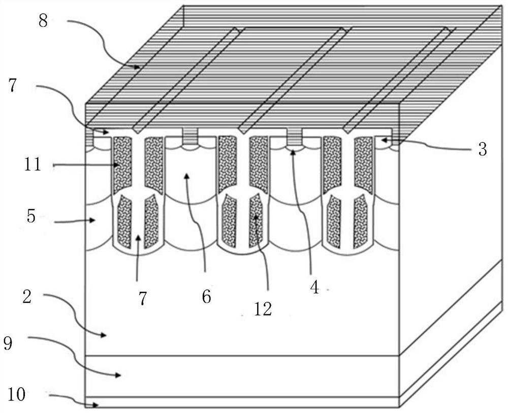
[0041] figure 2 It is a schematic structural diagram of a power semiconductor device with a split gate trench according to Embodiment 1. Such as figure 2 As shown, it may include: a semiconductor substrate 2, an N+ region 3, a P+ region 4, an N well region 5, a P well region 6, a plurality of stripe-shaped trench split polysilicon gates (including a polysilicon main gate 11, a polysilicon auxiliary gate 12 ), oxide layer 7, emitter metal layer 8, anode P region 9, and collector metal layer 10.

[0042] “Inside the surface of the semiconductor substrate 1 ” in this specification refers to a region extending downward from the surface of the semiconductor substrate 1 to a certain depth, which is a part of the semiconductor substrate 1 .

[0043] Wherein, the semiconductor substrate 2 may include semiconductor elements, such as silicon or silicon germanium of single crystal, polycrystalline or amorphous structure, or a mixed semiconductor structure, such as silicon carbide, al...

no. 2 example

[0058] Figure 5a It is a schematic structural diagram of a split-gate power semiconductor device with floating double-split dummy gates according to Embodiment 2 of the present invention, Figure 5b It is a schematic structural diagram of a split-gate power semiconductor device with double-split dummy gates grounded according to Embodiment 2 of the present invention. Such as Figure 5a As shown, it may include: a semiconductor substrate 2, an N+ region 3, a P+ region 4, an N well region 5, a P well region 6, a double-split dummy gate 17 of a stripe trench (comprising a polysilicon main dummy gate 171 and a polysilicon auxiliary dummy gate 171) gate 172), the true gate 13 split by the stripe trench (including the polysilicon main gate 131 and the polysilicon auxiliary gate 132), the oxide layer 7, the emitter metal layer 7, the anode P region 9, and the collector metal layer 10. The polysilicon main dummy gate 171 is a floating structure, which can change the input and outpu...

no. 3 example

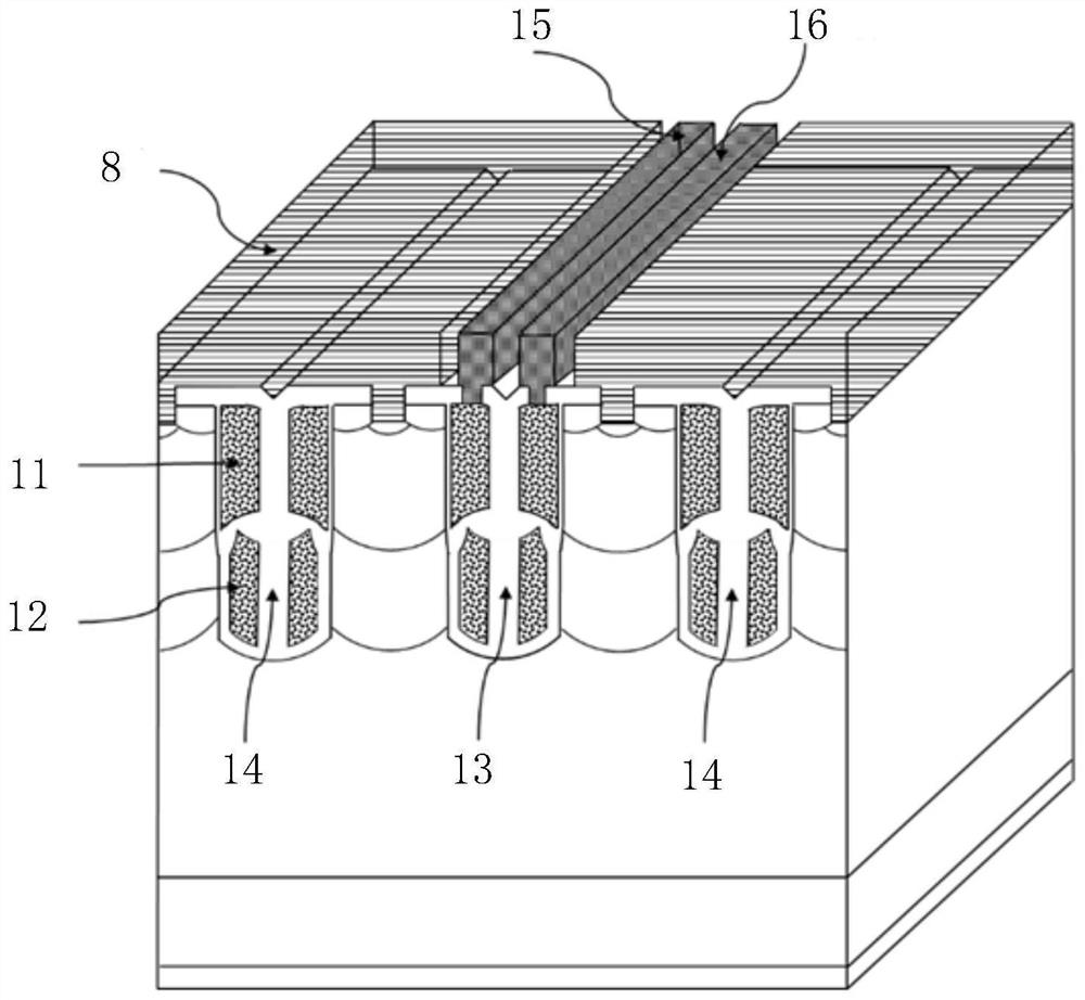
[0070] Figure 6 It is a schematic structural diagram of a double split gate power semiconductor device using an oxide layer with a uniform thickness according to another embodiment of the present invention, Figure 6 is a schematic structural diagram of a split-gate power semiconductor device according to Embodiment 3 of the present invention. Such as Figure 6As shown, it may include: a semiconductor substrate 2, an N+ region 3, a P+ region 4, an N well region 5, a P well region 6, and a stripe-shaped trench split-type true gate 13 (including a polysilicon main gate 131 and a polysilicon auxiliary gate 132) , double-split dummy gate 18 (including polysilicon main dummy gate 181 and polysilicon auxiliary dummy gate 182 ), oxide layer 7 , emitter metal layer 8 , anode P region 9 , and collector metal layer 10 . The polysilicon main dummy gate 181 is a floating structure, which changes the input and output capacitance of the trench power semiconductor device, thereby mediatin...


PUM


Abstract

The present invention discloses a split-gate trench power semiconductor device which comprises: an active region arranged on a semiconductor substrate, wherein the active region comprises a first well region and a second well region which are longitudinally stacked in the direction from the surface of the semiconductor substrate to the bottom of the semiconductor substrate; and one or more than one true gate grooves which are formed by etching and penetrate through the first well region and the second well region, wherein split type polycrystalline silicon true gates are arranged in the true gate grooves and comprise polycrystalline silicon main true gates and polycrystalline silicon auxiliary true gates, and the polycrystalline silicon main true gates and the polycrystalline silicon auxiliary true gates are arranged close to the tops and the bottoms of the grooves in a separated mode respectively. The polycrystalline silicon main true gates are control gates used for being connected with an external gate drive circuit, and the polycrystalline silicon main true gates and the polycrystalline silicon auxiliary true gates, the polycrystalline silicon true gates and the side wall of the true gate grooves and the polycrystalline silicon true gates and the bottom of the true gate grooves are isolated through interlayer media. According to the invention, the polysilicon gate in the strip-shaped groove is split to form the split gate, so that the stray capacitance is reduced, different electric connections are adopted, and the thickness of the oxide layer is set, so that the overall optimization of the chip performance is realized.

Description

technical field [0001] The invention relates to the technical field of power semiconductor devices, in particular to a split gate trench power semiconductor device. Background technique [0002] Insulated gate bipolar transistor (IGBT) is the only semiconductor device that combines MOSFET and bipolar transistor so far. It has the characteristics of high input impedance and fast response of MOSFET tube, and is widely used in rail transit, smart grid, electric Automobiles, new energy development and other fields. [0003] With the rapid development of IGBT technology, the trench gate can change the current channel from the surface horizontal to the vertical in the body, effectively eliminate the JFET effect in the planar gate body, and reduce the cell size so that the channel density is no longer limited by the chip surface area. The limit greatly increases the cell density, thereby greatly increasing the chip current density and reducing the chip on-state loss. However, as ...

Claims


Application Information

Patent Timeline
Patent Type & Authority Applications(China)
IPC IPC(8): H01L29/739H01L29/423H01L29/06
CPCH01L29/7393H01L29/42312H01L29/0684H01L29/423H01L29/739H01L29/06
Inventor 苏元宏王亚飞王彦刚戴小平覃荣震罗海辉
Owner ZHUZHOU CSR TIMES ELECTRIC CO LTD
Why Eureka
Try Eureka