Preparation method and application of nano-chain structure array

A nano-chain and micro-nano structure technology is applied in the field of preparation of nano-chain structure arrays, which can solve the problems of unsuitability for large-scale manufacturing of metal nano-structure arrays, limited local field enhancement effect, and expensive equipment, etc. Plasmonic effect, expanded application and industrialization prospects, high sensitivity effect

Pending Publication Date: 2021-05-14
JIANGSU UNIV OF TECH
View PDF6 Cites 1 Cited by
  • Summary
  • Abstract
  • Description
  • Claims
  • Application Information

AI Technical Summary

Problems solved by technology

[0005] In the prior art, the preparation methods of metal nanoparticle structure arrays include ion beam lithography, electron beam lithography, extreme ultraviolet lithography, nanoimprinting and other technologies. Although the prepared metal nanostructures have high resolution, precise size and shape, The periodicity is good, but

Method used


Image

  • Preparation method and application of nano-chain structure array
  • Preparation method and application of nano-chain structure array
  • Preparation method and application of nano-chain structure array

Examples


Embodiment 1

[0032] A photoresist layer with an array of striped hollow structures is prepared by wet etching:

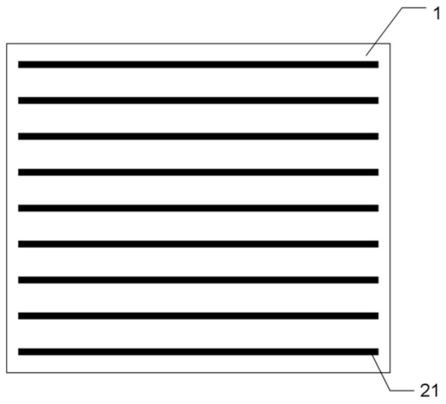
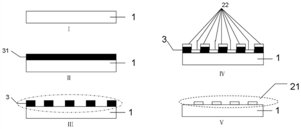
[0033] First, substrate 1, such as glass or conductive glass or silicon wafer, is thoroughly cleaned by detergents such as acetone, isopropanol, etc., to remove impurity ions (such as Figure 3-I );

[0034] Then spin-coat one deck positive photoresist film 31 (such as Figure 3-Ⅱ ), the thickness of the photoresist film is more than 200nm, after drying, a mask plate with a two-dimensional striped micro-nano structure array pattern is used for exposure, after exposure, post-baking and development are carried out, so that strips with strips are obtained on the surface of the substrate 1 The photoresist layer 3 of the hollow structure array (such as Figure 3-Ⅲ), the exposure process is to copy the pattern in the mask plate to the photoresist film 31.

[0035] In the above process, if the photoresist that is spin-coated is a positive photoresist, then the micro-nano structure a...

Embodiment 2

[0038] Preparation of strip-shaped hollow gold nanoarrays on the surface of the substrate:

[0039] The whole sample of the substrate 1 with the photoresist layer 3 of the strip-shaped hollow structure array in Example 1 is transferred to the thermal evaporation coating chamber, and the side with the photoresist layer 3 faces the evaporation source; the evaporation source material is selected For gold, the distance between the overall sample and the evaporation source is about 45cm, and the air in the thermal evaporation coating chamber is extracted to reduce the air pressure to 10 -4 Pascal; by heating the evaporation source, the evaporation material gold is converted into gold vapor and attached to the sample surface with a relatively low temperature (that is, there is gold on the substrate of the hollowed out area and the surface of the photoresist layer), and the deposition rate is 0.1nm / s, forming a layer of gold nanofilm 22 (such as Figure 3-Ⅳ );

[0040] Then the ab...

Embodiment 3

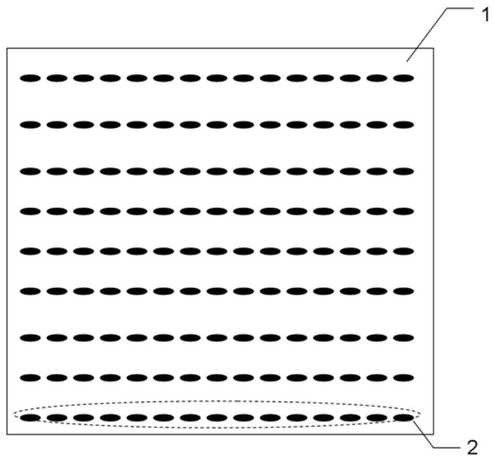
[0042] Preparation of nanochain structure arrays composed of gold nanoparticles as basic units:

[0043] Put the whole sample that has obtained the strip-shaped hollow gold nanoarray 21 on the surface of the substrate 1 through Example 2 into the annealing furnace (before putting into the annealing furnace, use a nitrogen gun to purge the sample several times to ensure that no dust is deposited on the sample. substrate), the vacuum degree of the annealing furnace was evacuated to 1×10 -2 Then, flow nitrogen gas into it, maintain normal pressure, heat the temperature in the furnace evenly to 450°C within 15 minutes by gradually heating, and keep it warm for 1 hour. After the heating, continue to flow nitrogen gas and cool it to room temperature. After completion, the annealing furnace was opened to remove the sample. The material is heated through the principle of relatively low melting point of nanomaterials in the annealing process, and then the surface tension of the metal ...


PUM

PropertyMeasurementUnit
Thicknessaaaaaaaaaa

Abstract

The invention relates to a preparation method and application of a nano-chain structure array. The preparation method comprises the following steps: (1) carrying out wet etching on the surface of a substrate to obtain a photoresist layer with a strip-shaped hollow structure array; (2) depositing on the substrate with the photoresist layer to obtain a gold nano-film, and then stripping the photoresist layer to obtain a strip-shaped hollow gold nano-array on the surface of the substrate; and (3) carrying out annealing treatment, and finally preparing the nano-chain structure array formed by taking gold nanoparticles as basic units on the substrate, wherein nano-chains are parallel to one another and the distance between the nano-chains is 200 nm-1000 nm, the basic unit of each nano-chain is the gold nanoparticles, and the distance between the gold nanoparticles is 2 nm-10 nm. The method provided by the invention is low in production cost and is suitable for large-scale production; and the nano-chain structure array provided by the invention is applied to a surface enhanced Raman scattering substrate, so that the surface plasmon polariton effect can be improved and the local field enhancement effect is improved.

Description

technical field [0001] The invention relates to the technical field of nanomaterial preparation, in particular to a preparation method and application of a nanochain structure array. Background technique [0002] It is generally described as a charged system in which positive and negative charges are separated in a high-temperature molten state as a plasmonic system, and plasmons are the collective oscillation quantum of the plasmonic system. When studying conductors and metal substances, the electrons inside can be approximated as free electrons in the background of positive charges, so that conductors and metal substances can also be treated as plasma systems equivalently. In view of the roaming characteristics of valence electrons, there must be an electron density fluctuation in the small range of electron movement in the conductor and metal material systems. Due to the long-range nature of the Coulomb interaction, the correlation of electron motion will evolve the fluc...

Claims


Application Information

Patent Timeline
IPC IPC(8): C23C14/04C23C14/35C23C14/24C23C14/58G01N21/65
CPCC23C14/042C23C14/35C23C14/24C23C14/5806G01N21/658
Inventor 朱圣清向萌许郅博周春鹤
Owner JIANGSU UNIV OF TECH
Why Eureka
Try Eureka