Semiconductor high-density lead frame and its manufacturing process

A lead frame and manufacturing process technology, applied in semiconductor/solid-state device manufacturing, semiconductor devices, semiconductor/solid-state device components, etc., can solve the problems of low lithography pattern accuracy, easy appearance of burrs, and inconvenient lead frame processing and manufacturing.

Active Publication Date: 2022-02-11
昆山弗莱吉电子科技有限公司
View PDF4 Cites 0 Cited by
  • Summary
  • Abstract
  • Description
  • Claims
  • Application Information

AI Technical Summary

Problems solved by technology

[0003] Nowadays, the processing methods of lead frames include die stamping method and chemical etching method. Among them, the die stamping method has high production efficiency, but the processing accuracy is difficult to guarantee, and the appearance is prone to burrs during processing, which has been gradually eliminated by us; Etching is a more commonly used processing method, but there are still many disadvantages in the processing process of the existing etching method, such as low precision of photolithographic patterns, side corrosion and other problems, which are very important in the process of lead frame manufacturing. bring inconvenience

Method used


Image

  • Semiconductor high-density lead frame and its manufacturing process
  • Semiconductor high-density lead frame and its manufacturing process

Examples


Embodiment 1

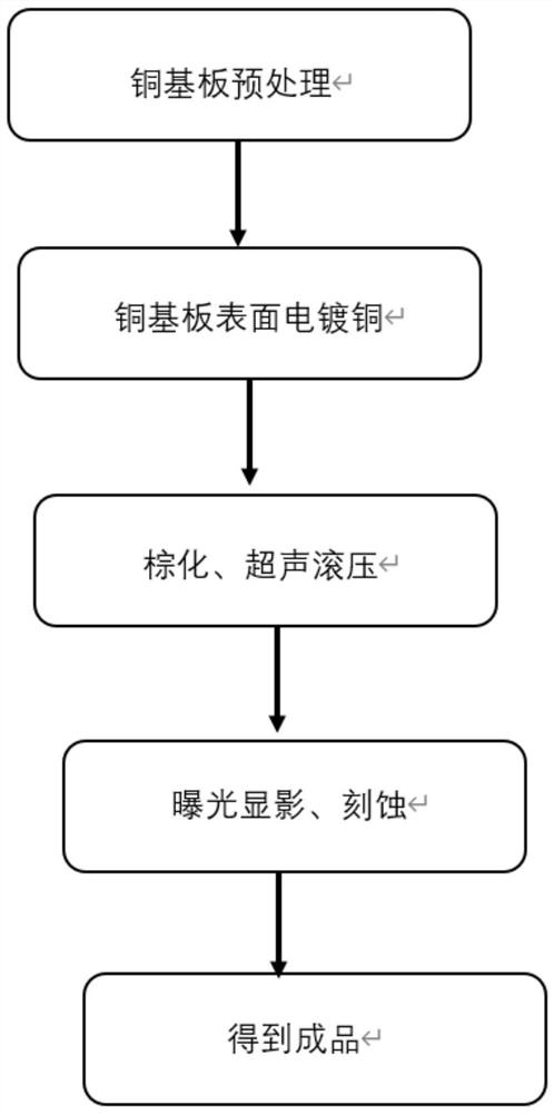
[0042] A manufacturing process for a semiconductor high-density lead frame, comprising the following steps:

[0043] (1) Take the copper substrate, wash it with deionized water for 3 minutes, then place it in the electrolyte for cathodic electrolytic degreasing, rinse it with deionized water, then soak it in nitric acid solution for 20s, remove the surface oxide film, rinse it with deionized water, and place it Activated in the activation solution for 3 minutes, rinsed with deionized water to obtain a pretreated copper substrate; the electrolyte is a mixture of trisodium phosphate, sodium hydroxide, sodium silicate and sodium carbonate, the temperature during electrolytic degreasing is 50°C, and the current The density is 10A / dm 2 , The electrolytic oil removal time is 20s.

[0044] (2) Take the pretreated copper substrate, place it in the electroplating solution, and electroplate a pure copper layer on the surface of the pretreated copper substrate, the electroplating temper...

Embodiment 2

[0051] A manufacturing process for a semiconductor high-density lead frame, comprising the following steps:

[0052] (1) Take the copper substrate, wash it with deionized water for 4 minutes, then place it in the electrolyte for cathodic electrolytic degreasing, rinse it with deionized water, and then soak it in nitric acid solution for 25s to remove the surface oxide film, rinse it with deionized water and place it Activated in the activation solution for 4 minutes, rinsed with deionized water, and obtained the pretreated copper substrate; the electrolyte was a mixture of trisodium phosphate, sodium hydroxide, sodium silicate and sodium carbonate, and the temperature during electrolytic degreasing was 52°C, and the current The density is 11A / dm 2 , The electrolytic oil removal time is 23s.

[0053] (2) Take the pretreated copper substrate, place it in the electroplating solution, and electroplate a pure copper layer on the surface of the pretreated copper substrate, the elec...

Embodiment 3

[0060] A manufacturing process for a semiconductor high-density lead frame, comprising the following steps:

[0061] (1) Take the copper substrate, wash it with deionized water for 5 minutes, then place it in the electrolyte for cathodic electrolytic degreasing, rinse it with deionized water, and then soak it in nitric acid solution for 30s to remove the surface oxide film, rinse it with deionized water and place it Activated in the activation solution for 5 minutes, rinsed with deionized water to obtain a pretreated copper substrate; the electrolyte is a mixture of trisodium phosphate, sodium hydroxide, sodium silicate, and sodium carbonate, and the temperature during electrolytic degreasing is 55°C. The density is 12A / dm 2 , The electrolytic oil removal time is 25s.

[0062] (2) Take the pretreated copper substrate, place it in the electroplating solution, and electroplate a pure copper layer on the surface of the pretreated copper substrate, the electroplating temperature ...


PUM


Abstract

The invention discloses a semiconductor high-density lead frame and its manufacturing process, which includes steps such as pretreatment, electroplating, browning, rolling, and photolithography to prepare a high-density, high-precision semiconductor lead frame. The application firstly carries out surface treatment on the copper substrate, and first puts the copper substrate in the electrolyte for cathodic electrolytic degreasing to remove the oil on the surface of the copper substrate and ensure that the surface of the copper substrate is clean; then put it in an acid solution, this step is to thoroughly Remove the oxide film on the surface of the copper substrate; then perform surface activation on the copper substrate to maintain the surface activity of the copper substrate, so that the copper substrate and the subsequent plating layer can be well bonded to obtain a pretreated copper substrate. After the photolithography of the application, a photolithographic pattern is formed on the surface of the copper substrate. In actual operation, the subsequent electroplating metal layer, chip bonding and other processes can be carried out. The surface of the prepared lead frame is free of scratches, dents and stains, and can be widely used. In the direction of chip packaging and so on.

Description

technical field [0001] The invention relates to the technical field of lead frames, in particular to a semiconductor high-density lead frame and a manufacturing process thereof. Background technique [0002] As the chip carrier of integrated circuits, the lead frame is a key structural part that realizes the electrical connection between the lead-out end of the chip's internal circuit and the outer lead by means of bonding materials (gold wire, aluminum wire, copper wire) to form an electrical circuit. When it comes to the bridge function of connecting with external wires, most semiconductor integrated blocks need to use lead frames, which are important basic materials in the electronic information industry. [0003] Nowadays, the processing methods of lead frames include die stamping method and chemical etching method. Among them, the die stamping method has high production efficiency, but the processing accuracy is difficult to guarantee, and the appearance is prone to bur...

Claims


Application Information

Patent Timeline
Patent Type & Authority Patents(China)
IPC IPC(8): H01L21/48H01L23/495C25D3/28C25D5/34C25F1/04C23C22/52C23C22/82C23F1/02B05D3/02B05D7/14
CPCH01L21/4821H01L21/4842H01L21/4828H01L21/4835H01L23/49586B05D7/14B05D3/0254C25D3/28C25D5/34C25F1/04C23C22/52C23C22/82C23F1/02
Inventor 周武刘波
Owner 昆山弗莱吉电子科技有限公司
Why Eureka
Try Eureka