Full-printed semiconductor carbon nanotube field effect transistor and preparation method thereof

A technology of field-effect transistors and carbon nanotubes, which is applied in semiconductor/solid-state device manufacturing, semiconductor devices, nanotechnology, etc., can solve the problem that printing electronic ink is not easy to store, and it is impossible to realize single-chiral carbon nanotubes and printing equipment. Problems such as blockage

Pending Publication Date: 2021-07-30
UNIV OF ELECTRONICS SCI & TECH OF CHINA
View PDF8 Cites 1 Cited by
  • Summary
  • Abstract
  • Description
  • Claims
  • Application Information

AI Technical Summary

Problems solved by technology

[0006] (1) The existing process cannot realize the preparation of monochiral carbon nanotubes. The obtained carbon nanotubes are a mixture of different tube diameters and chiral distributions, which contain both metallic and multiple chiral semiconducting carbons. Nanotubes, and device manufacturing usually only requires carbon nanotubes with a single conductive property;
[0007] (2) Due to the large π bond between carbon nanotubes, the strong van der Waals force (the van der Waals force between adjacent nanotubes is about 500eV / μm), and the entanglement formed by the large aspect ratio of carbon nanotubes , causing nanotubes to easily aggregate into bundles or exist in the form of aggregates in the solution, so the printed electronic ink prepared by using carbon nanotubes is not easy to store and is likely to cause blockage of printing equipment, which is difficult to form with the flexible printing process good compatibility;

Method used


Image

  • Full-printed semiconductor carbon nanotube field effect transistor and preparation method thereof
  • Full-printed semiconductor carbon nanotube field effect transistor and preparation method thereof
  • Full-printed semiconductor carbon nanotube field effect transistor and preparation method thereof

Examples


Embodiment 1

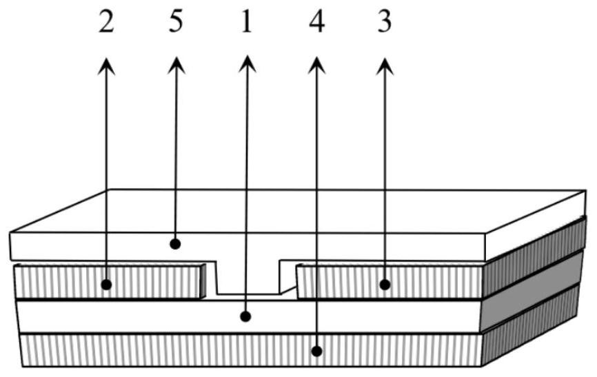
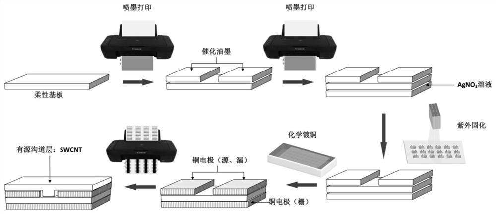
[0039] like figure 2 Shown is the preparation method of the fully printed flexible high-purity semiconductor single-walled carbon nanotube field-effect transistor in this embodiment, including the following steps:

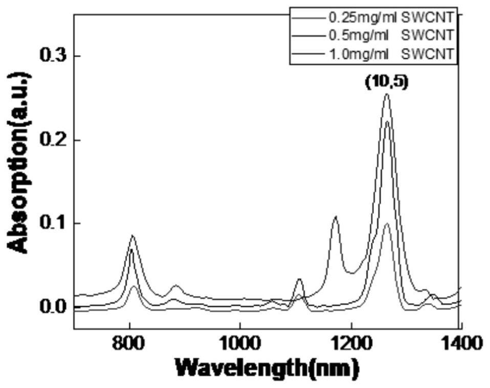
[0040] 1) Preparation of high-purity dispersion enriched with semiconducting carbon nanotubes: Weigh 10 mg of fluorenyl conjugated polymer poly[(9,9-dioctylfluorenyl-2,7-diyl)-alt-( Benzo[2,1,3]thiadiazole 4,8-diyl)] was dissolved in 20ml of organic solvent toluene, the beaker was wrapped with tinfoil paper to protect from light, and magnetically stirred for 10 minutes to fully dissolve to form a mixed solution . Weigh 10 mg of SWCNT and add it to the mixed solution, and then carry out liquid-phase ultrasonic stripping in a low-temperature water bath (200W, 40kHz). The treatment time is 60-90 minutes, and the temperature is kept at 0°C. Fluorene-based conjugated polymers provide sufficient selective coating of single-walled carbon nanotubes. Take out the sample...

Embodiment 2

[0044] The source, drain, and gate metal electrode arrays are integratedly prepared by selecting a solution two-step method, and a fully printed flexible high-purity semiconducting single-walled carbon nanotube field-effect transistor is prepared.

[0045] Preparation of source, drain, and gate electrode metal layers of transistors by solution two-step method: Taking the preparation of copper metal layer as an example, first print Ag on the flexible substrate by solution two-step method + Catalytic precursor, the front is a patterned source and drain electrode array, and the back is a full-surface back gate electrode. After UV curing to form a cured ink film of the precursor, the substrate is completely immersed in the prepared electroless copper plating agent. The temperature of the reaction environment is set to 50° C., and the reaction time is 10 minutes to complete the preparation of the source / drain / gate electrode arrays on the front and back sides of the substrate. The r...


PUM

PropertyMeasurementUnit
carrier mobilityaaaaaaaaaa
thicknessaaaaaaaaaa
thicknessaaaaaaaaaa

Abstract

The invention belongs to the technical field of semiconductor devices, and particularly relates to a full-printed semiconductor carbon nanotube field effect transistor and a preparation method thereof. The transistor comprises a bottom gate electrode (4), an insulated gate dielectric layer (1), a source electrode (2), a drain electrode (3) and a source semiconductor channel layer (5) from bottom to top. The preparation method comprises the following steps: firstly, preparing a high-purity dispersion liquid which is suitable for an ink-jet printing process and is enriched with semiconductor carbon nanotubes; a source electrode (2) and a drain electrode (3) are prepared on the front surface of the flexible substrate, and a large-area back gate electrode (4) is prepared on the back surface of the flexible substrate; and finally, a layer of single-walled carbon nanotube ink is printed on the source electrode and the drain electrode through an ink-jet printing process to serve as an active semiconductor channel layer (5) so as to complete the full-printing preparation of the flexible semiconductor single-walled carbon nanotube field effect transistor. Based on the technical means of high-selectivity purification of the carbon nanotubes, full-printing preparation of the field effect transistor and the like, the manufacturing method of the carbon nanotube field effect transistor, which is simple, efficient and easy for large-scale preparation, is provided, and the obtained flexible transistor device has the characteristics of excellent electrical properties and bending and stretching resistance.

Description

technical field [0001] The invention belongs to the technical field of semiconductor devices, and in particular relates to a fully printed semiconducting carbon nanotube field effect transistor and a preparation method thereof. Background technique [0002] The traditional integrated circuit chip IC, including the printed circuit board PCB, is processed through a series of complex processes such as photolithography, development, and etching. Not only is the process flow complicated, but the cost is expensive and wastes consumables. It is also very high, so the development of printed electronics is particularly important for the manufacture of electronic devices. As a green and consumable-saving manufacturing technology, printed electronics technology can directly reduce the complexity of the preparation process and improve the utilization rate of raw materials by directly printing the required patterns on the printing substrate. Flexible and efficient tuning of electrical p...

Claims


Application Information

Patent Timeline
Patent Type & Authority Applications(China)
IPC IPC(8): H01L51/05H01L51/40H01L51/30B82Y40/00B82Y30/00
CPCB82Y40/00B82Y30/00H10K71/135H10K71/20H10K71/311H10K71/60H10K85/221H10K10/484H10K10/466
Inventor 冯哲圣廖小涵王莉婷王焱
Owner UNIV OF ELECTRONICS SCI & TECH OF CHINA
Why Eureka
Try Eureka