Nanosecond, picosecond and femtosecond beam combination laser parallel finishing and polishing machining method
A processing method, femtosecond technology, applied in the field of additive manufacturing, can solve problems such as low efficiency, high cost, and poor quality
- Summary
- Abstract
- Description
- Claims
- Application Information
AI Technical Summary
Problems solved by technology
Method used
Image

Examples
Embodiment 1
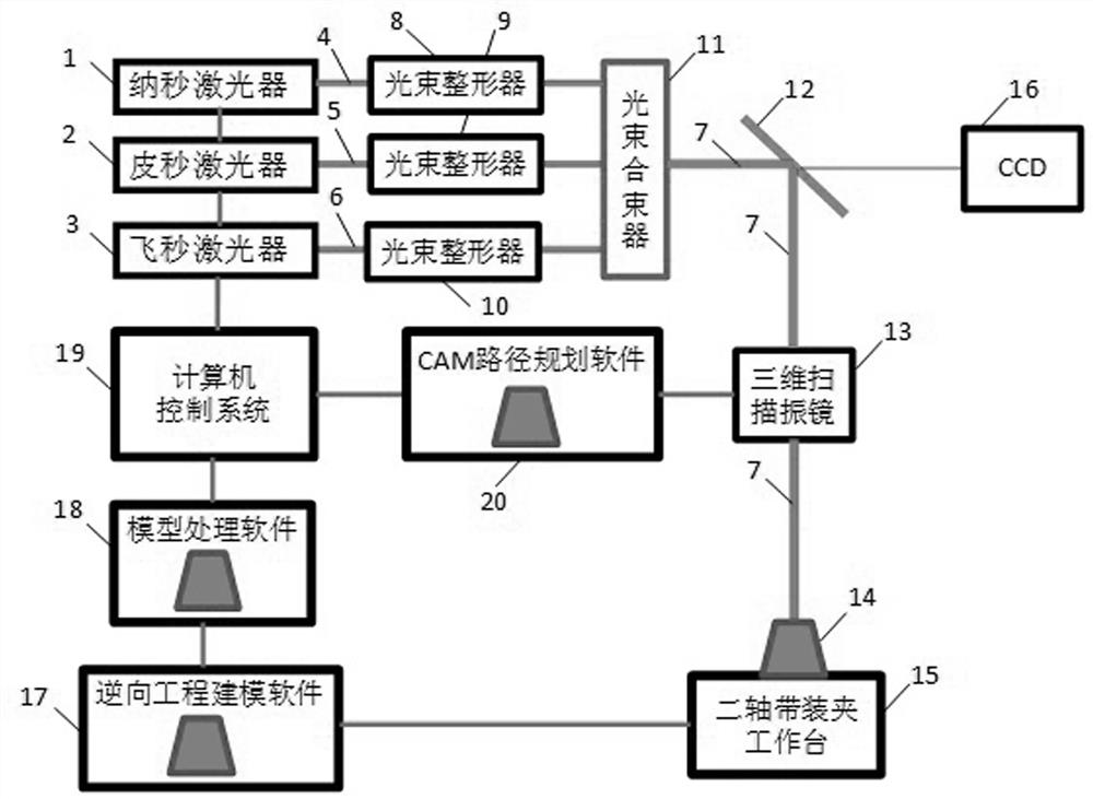
[0040] 1. Install the metal additive manufacturing parts 14 of TC4 alloy on the two-axis belt clamping workbench 15, and put the whole device in an argon inert gas sealed cabin, the oxygen and water content in the sealed cabin is ≤50ppm, the purpose It is to prevent the metal from being oxidized and polluted by the air; the digital model of the metal additive manufacturing part 14 of the TC4 alloy is established by reverse engineering modeling software, and compared with the shape and size of the three-dimensional model of the actual metal additive manufacturing part 14, through The model processing software determines the machining allowance of the metal additive manufacturing parts 14 of the TC4 alloy, and the machining allowance is determined to be about 800 μm;
[0041] 2. Through the CAM path planning software 20, the machining allowance path of the metal additive manufacturing parts 14 of the TC4 alloy is transmitted to the three-dimensional scanning galvanometer 13 and t...
Embodiment 2
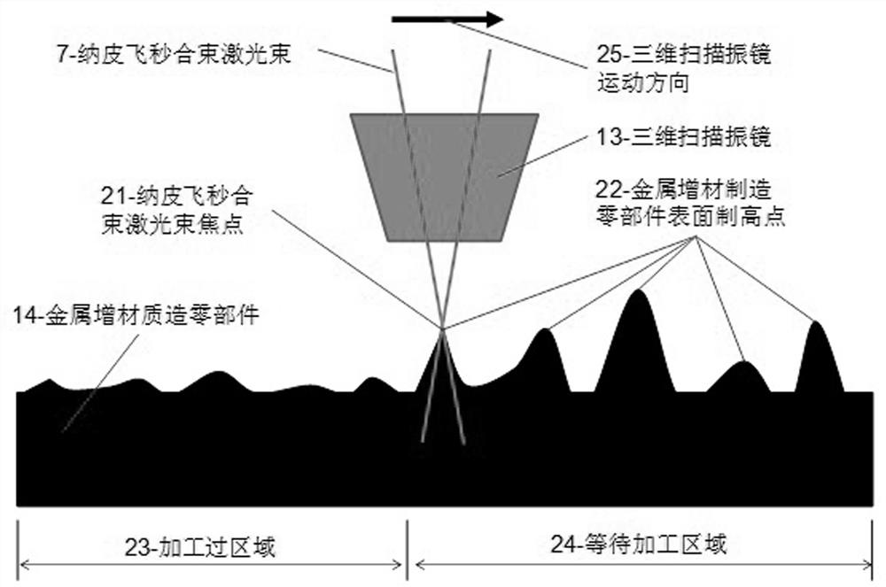
[0047] The TC4 alloy in embodiment 1 is replaced by nickel-based superalloy, and the method is the same as in embodiment 1. The scanning speed of the three-dimensional scanning galvanometer 13 is 120m / min; the high energy density of the nanopicosecond combined laser beam 7 is used to combine the principle of evaporation and melting of the metal, and the focus of the nanopicosecond combined laser beam 7 Irradiate the metal additive manufacturing parts of nickel-based superalloy 14 to the commanding heights of the surface of the machining allowance, so that the metal at the commanding heights of the surface evaporates and melts. After the first layer is completed, the second layer is cycled, and so on for the twelfth cycle. Layer, realized the metal additive manufacturing parts of nickel-based superalloys, the subsequent processing thickness (depth) ≈ 50 μm, and the processing allowance was determined to be about 600 μm; the processing efficiency ≈ 10cm 2 / min, surface roughnes...
PUM
| Property | Measurement | Unit |
|---|---|---|
| power | aaaaa | aaaaa |
| wavelength | aaaaa | aaaaa |
| wavelength | aaaaa | aaaaa |
Abstract
Description
Claims
Application Information
PatSnap Eureka turns technology decisions into work you can execute. Powered by our Innovation Knowledge Graph, it runs expert workflows across engineering, life sciences, materials and intellectual property. Get your review-ready output in minutes.


