A method for preparing tungsten trioxide high light extraction efficiency OLED external light extraction layer by ultrasonic spraying
A technology of ultrasonic spraying and highlight extraction, which is applied in semiconductor/solid-state device manufacturing, semiconductor devices, electrical components, etc., can solve the problems of low output coupling efficiency of OLED external light, high technical cost and difficulty, and achieve low cost and large size Effects of large-scale loading, low material cost, and lower deposition temperature
- Summary
- Abstract
- Description
- Claims
- Application Information
AI Technical Summary
Problems solved by technology
Method used
Image
Examples
preparation example Construction
[0049] The preparation method steps are as follows:
[0050] Step 1: Clean the glass substrate sequentially by ultrasonic cleaning for 15 minutes with decontamination agent, deionized water and absolute ethanol respectively.
[0051] Step 2: Dry the glass substrate in an oven at 200° C. for 1 hour, load the dried glass substrate on a glass stage, and heat the stage to 600° C., and then keep it for 10 minutes.
[0052] Step 3: Ultrasonic cleaning of the glass substrate for 15 minutes was performed sequentially with decontamination agent, deionized water, acetone, deionized water and isopropanol respectively.
[0053] Step 4: Pass the glass substrate into the vacuum evaporation chamber to evaporate Au / TAPC / TAPC:P0-T2T:FIrpic(1:1,15%,20nm) / P0-T2T / LiF / Au sequentially; the organic layer evaporation rate for The evaporation rate of the inorganic layer is
Embodiment 1
[0054] Device 1 (Device 1) was prepared in Example 1.
Embodiment 2
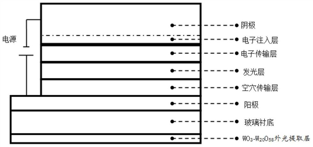
[0056] The device structure from bottom to top is as follows:
[0057] WO 3 -W 20 o 58 -1 / glass substrate / Au(120nm) / TAPC(35nm) / TAPC:P0-T2T:FIrpic(1:1,15%,20 nm) / P0-T2T(50nm) / LiF(1nm) / Au( 100nm)
[0058] Namely: the external light extraction layer of Experiment 1, the thickness of the anode is 120nm, the thickness of the hole transport layer is 35nm, the thickness of the light emitting layer is 20nm, the thickness of the electron transport layer is 50nm, the thickness of the electron injection layer is 1nm, and the thickness of the cathode is 100nm.
[0059] The preparation method steps are as follows:
[0060] Step 1: get 53.5g ammonium paratungstate, ethylene glycol butyl ether (dipole moment is 6.94 10 -30 cm) 500mL and 9.5% volume fraction ratio of dilute ammonia 500mL are mixed to obtain a precursor solution that is a mixed solution of ammonium tungstate with a concentration of 53.5g / L.
[0061] Step 2: Use decontamination agent, deionized water, and absolute ethanol...
PUM
| Property | Measurement | Unit |
|---|---|---|
| diameter | aaaaa | aaaaa |
| thickness | aaaaa | aaaaa |
| thickness | aaaaa | aaaaa |
Abstract
Description
Claims
Application Information


