

Method for manufacturing conductive pattern by selectively activating insulating material through laser and chemical combination
A technology of chemical bonding and conductive pattern, applied in conductive pattern formation, printed circuit manufacturing, electrical components, etc., can solve the problems of low cost performance of lasers, low photon energy, increased difficulty, etc., and achieve good control of plating effect and processing range. Large, good processing consistency
- Summary
- Abstract
- Description
- Claims
- Application Information
AI Technical Summary
Problems solved by technology
Method used
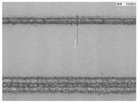
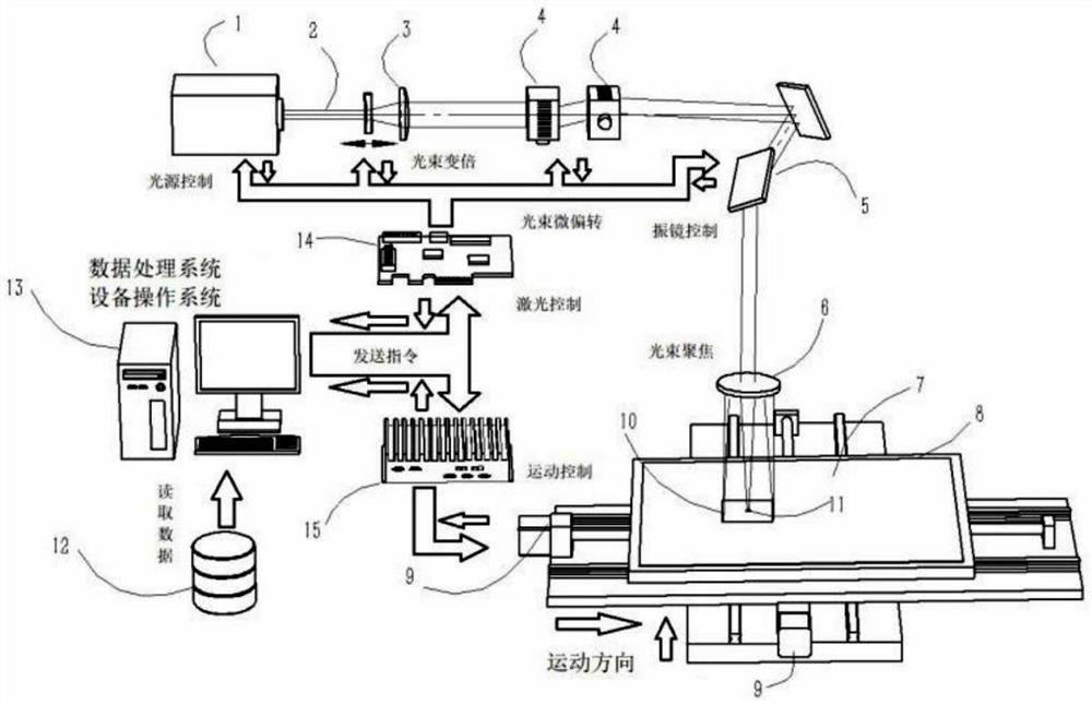
Image

Examples
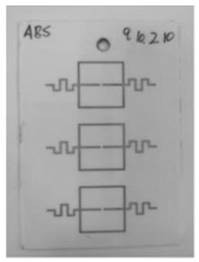
Embodiment 1
[0125] (1) Determine the upper limit of chemical treatment parameters of ABS material and the lower limit of laser processing intensity.
[0126]Starting from the process conditions of ABS plastic electroless plating, first confirm the chemical treatment steps of one of the processes: degreasing - pre-dipping - activation - debonding - electroless copper deposition. In this example:
[0127] ①It is preferable to use an alkaline degreaser for degreasing. The solution composition is: sodium carbonate 15g / L, sodium phosphate 30g / L, sodium hydroxide 50g / L, surfactant 2g / L, temperature 50~80℃, time 5~ 10min.
[0128] ②Pre-impregnation-activation-debonding, wherein the pre-impregnated solution composition is: hydrochloric acid 200ml / L, room temperature, time 1~3min; the activated solution composition is: palladium chloride 0.05g / L, stannous chloride 10g / L , hydrochloric acid 200ml / L, sodium chloride 50g / L, temperature 25~35℃, time 1~5min; the solution composition of degumming is: ...
Embodiment 2
[0157] (1) Determine the upper limit of chemical treatment parameters of ABS+40%PC material and the lower limit of laser processing intensity.
[0158] The chemical properties of ABS+PC and ABS materials are similar, and the plastic electroless plating process is similar to the process steps of ABS, specifically: degreasing-chemical roughening-prepreg-activation-debonding-chemical copper precipitation. In an example:
[0159] ①It is preferable to use an alkaline degreaser for degreasing. The solution composition is: sodium carbonate 15g / L, sodium phosphate 30g / L, sodium hydroxide 50g / L, surfactant 2g / L, temperature 50~80℃, time 5~ 10min.
[0160] ②The composition of the chemical roughening solution is: sulfuric acid 220ml / L, temperature 65~80℃, time 10~30min.
[0161] ③Pre-soak-activation-debonding, wherein the pre-soak solution composition is: hydrochloric acid 200ml / L, room temperature, time 1~3min; the activated solution composition is: palladium chloride 0.05g / L, stannou...
Embodiment 3
[0188] (1) Determine the upper limit of the chemical processing parameters of the LCP material and the lower limit of the laser processing intensity.
[0189] Starting from the process conditions of ABS plastic electroless plating, first confirm the chemical treatment steps of one of the processes: degreasing - pre-dipping - activation - debonding - electroless copper deposition. In this example:
[0190] ①It is preferable to use an alkaline degreaser for degreasing. The solution composition is: sodium carbonate 15g / L, sodium phosphate 30g / L, sodium hydroxide 50g / L, surfactant 2g / L, temperature 50~80℃, time 5~ 10min.
[0191] ②Pre-impregnation-activation-debonding, wherein the pre-impregnated solution composition is: hydrochloric acid 200ml / L, room temperature, time 1~3min; the activated solution composition is: palladium chloride 0.05g / L, stannous chloride 10g / L , hydrochloric acid 200ml / L, sodium chloride 50g / L, temperature 25~35℃, time 1~5min; the solution composition of ...
PUM
| Property | Measurement | Unit |
|---|---|---|
| Wavelength | aaaaa | aaaaa |
Abstract
Description
Claims
Application Information