Optical PUF as well as preparation method and application thereof
An optical and metal technology, applied in the security field based on PUF, can solve problems such as non-compliance, expensive preparation, nanoparticle distribution adhesion, poor mechanical stability, etc., and achieve density control, high randomness and complexity , good mechanical and thermal stability
- Summary
- Abstract
- Description
- Claims
- Application Information
AI Technical Summary
Problems solved by technology
Method used
Image

Examples
preparation example Construction
[0031] The invention provides a kind of preparation method of optical PUF, comprises the following steps:
[0032] A) depositing the first metal on the substrate to obtain the first metal layer;
[0033] B) depositing a second metal on the first metal layer to obtain a second metal layer;
[0034] C) annealing the composite layer obtained in step B) to form core-shell nanoparticles to obtain an optical PUF.
[0035] In the present invention, the first metal is deposited on the base to obtain the first metal layer.
[0036] In some embodiments of the present invention, the material of the substrate includes at least one of silicon, gallium arsenide, aluminum gallium nitride, gallium nitride, zinc oxide, gallium oxide, indium phosphide and silicon carbide.
[0037] In some embodiments of the invention, the base is composited on a substrate. The substrate can be sapphire. The present invention has no special limitation on the thickness of the substrate.
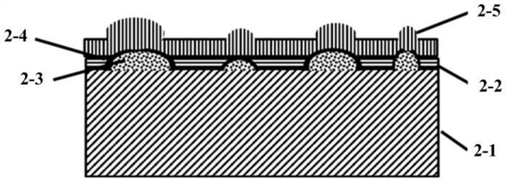
[0038] In some embo...
Embodiment 1
[0094] Preparation of GaN APD device electrode optical PUF:
[0095] 1) Using MOCVD to epitaxially grow GaN p-i-n structures on sapphire substrates, including 600nm n-GaN layers, 200nm unintentionally doped i-GaN layers, 100nm p-GaN layers, and 20nm p+GaN layers to facilitate the formation of ohmic contacts , to obtain a substrate with a thickness of 500 μm including sapphire;
[0096] 2) Depositing a 2nm titanium material on the p-GaN layer by electron beam evaporation by magnetron sputtering to obtain the first metal layer;
[0097] 3) Depositing an 8nm gold material on the first metal layer by magnetron sputtering to obtain a second metal layer;
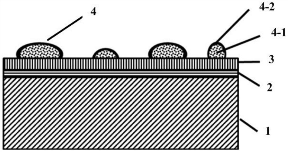
[0098] 4) Perform rapid annealing, the annealing temperature is 600°C, the annealing time is 3min, the annealing atmosphere includes oxygen and nitrogen, the volume ratio of oxygen and nitrogen is 1:5; core-shell nanoparticles are formed; the structure is as figure 1 shown;
[0099] 5) Plasma enhanced chemical vapor deposition ...
Embodiment 2
[0106] Preparation of GaAs device electrode optical PUF:
[0107] 1) The GaAs p-i-n structure is epitaxially grown on the sapphire substrate by MOCVD, including a 600nm n-GaAs layer, a 200nm unintentionally doped i-GaAs layer and a 100nm p-GaAs layer to promote the formation of ohmic contacts, and obtain a sapphire substrate with a thickness of 600μm substrate;
[0108] 2) Depositing 5nm titanium material on the p-GaAs layer by magnetron sputtering to obtain the first metal layer;
[0109] 3) Depositing a 10nm gold material by magnetron sputtering on the first metal layer to obtain a second metal layer;
[0110] 4) Perform rapid annealing, the annealing temperature is 620°C, the annealing time is 2min, the annealing atmosphere includes oxygen and nitrogen, the volume ratio of oxygen and nitrogen is 1:4; core-shell nanoparticles are formed;
[0111] 5) Depositing 300nm of gold by magnetron sputtering to obtain a third metal layer for forming an ohmic contact electrode with go...
PUM
| Property | Measurement | Unit |
|---|---|---|
| Thickness | aaaaa | aaaaa |
| Thickness | aaaaa | aaaaa |
| Thickness | aaaaa | aaaaa |
Abstract
Description
Claims
Application Information
 - Generate Ideas
- Intellectual Property
- Life Sciences
- Materials
- Tech Scout
- Unparalleled Data Quality
- Higher Quality Content
- 60% Fewer Hallucinations
Browse by: Latest US Patents, China's latest patents, Technical Efficacy Thesaurus, Application Domain, Technology Topic, Popular Technical Reports.
© 2025 PatSnap. All rights reserved.Legal|Privacy policy|Modern Slavery Act Transparency Statement|Sitemap|About US| Contact US: help@patsnap.com