


Quick Research
Generate reliable direction feasibility study reports for your R&D in just a few steps.

Technical Q&A
Discover and master advanced knowledge NOW. Basics, ideas, possibilities, all at once.

Find Solutions
As an expert in R&D theories, this can generate solutions to your technical problems instantly.

Evaluate Feasibility
Analyze your overall solution with one click, know your potential R&D risks in advance.

Monitor Landscape
Get weekly tech updates, stay abreast of the latest tech innovations and key insights.
Trans-flexible perovskite solar cell and preparation method thereof
A solar cell and perovskite technology, applied in circuits, photovoltaic power generation, electrical components, etc., can solve the problems of being unsuitable for flexible perovskite solar cells and poor performance of flexible perovskite solar cells, and achieve high photoelectric conversion efficiency , high open circuit voltage Voc, and good long-term stability
- Summary
- Abstract
- Description
- Claims
- Application Information
AI Technical Summary
Problems solved by technology
Method used
Image

Examples
Embodiment 1
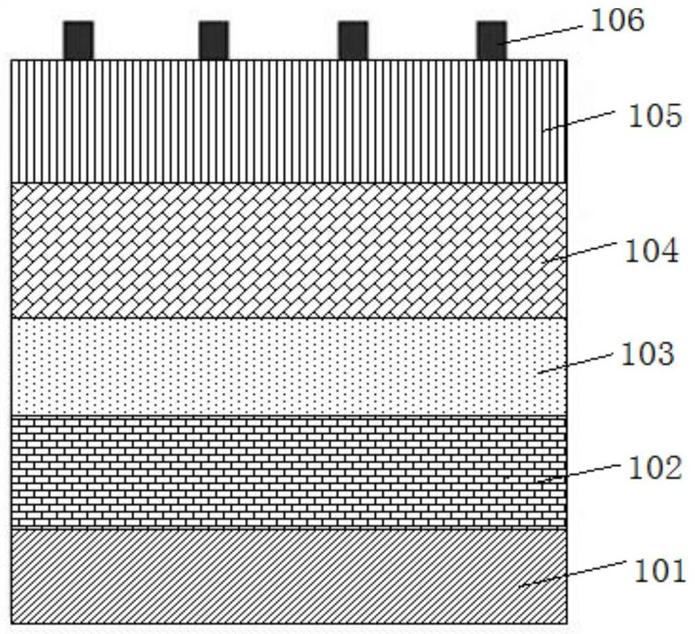
[0047] Step 1, flexible substrate pretreatment
[0048] Wash the cut 15*20cm flexible substrate in deionized water for 30 minutes, put it in a clean oven to dry, and obtain the cleaned flexible substrate, which is made of PI material;
[0049] Step 2, preparing a conductive film electrode layer on the cleaned flexible substrate
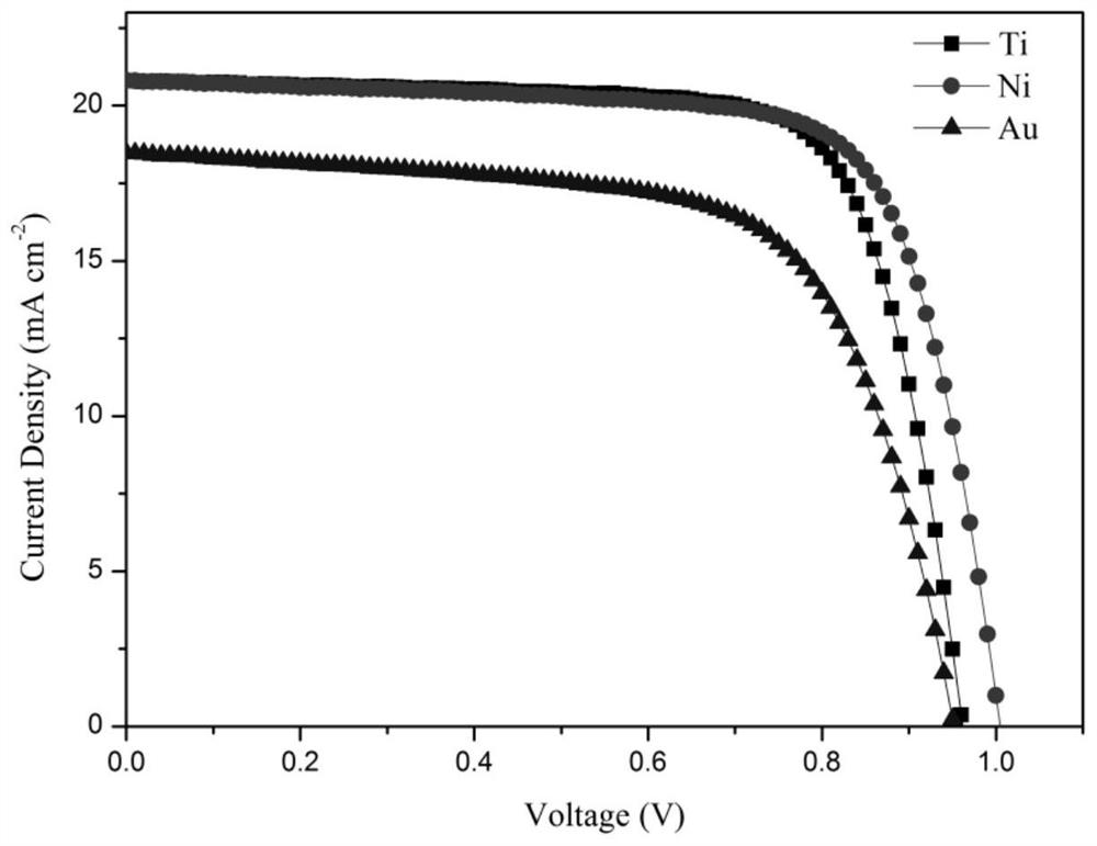
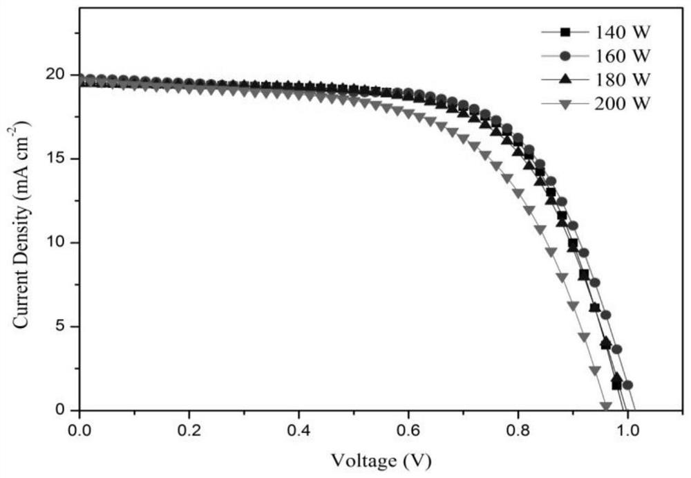
[0050]Metallic nickel was plated on the flexible substrate by electron beam evaporation with a thickness of 200nm, and the conductive metal oxide ITO was sputtered onto the metal layer with a power of 180W by magnetron sputtering;
[0051] Step 3, preparing a hole transport layer film on the conductive film electrode
[0052] Nickel oxide hole transport layer thin film is plated on the conductive substrate by electron beam evaporation method, the thickness is 15nm;
[0053] Step 4, preparing a perovskite light-absorbing layer film on the hole transport layer film
[0054] The 1.4M perovskite precursor solution was composed of FAI, PbI 2 , MABr, Pb...
Embodiment 2
[0060] Step 1, flexible substrate pretreatment
[0061] Wash the cut 15*20cm flexible substrate in deionized water for 30 minutes, put it in a clean oven to dry, and obtain the cleaned flexible substrate, which is made of PI material;
[0062] Step 2, preparing a conductive film electrode layer on the cleaned flexible substrate
[0063] Metal titanium is plated on the flexible substrate by electron beam evaporation method with a thickness of 200nm, and the conductive metal oxide ITO is sputtered onto the metal layer with a power of 180W by magnetron sputtering method;
[0064] Step 3, preparing a hole transport layer film on a conductive substrate
[0065] Nickel oxide hole transport layer thin film is plated on the conductive substrate by electron beam evaporation method, the thickness is 15nm;
[0066] Step 4, preparing a perovskite light-absorbing layer film on the hole transport layer film
[0067] The 1.4M perovskite precursor solution was composed of FAI, PbI 2 , MAB...
Embodiment 3
[0073] Step 1, flexible substrate pretreatment
[0074] Wash the cut 15*20cm flexible substrate in deionized water for 30 minutes, put it in a clean oven to dry, and obtain the cleaned flexible substrate, which is made of PI material;
[0075] Step 2, preparing a conductive film electrode layer on the cleaned flexible substrate
[0076] Metal gold was plated on the flexible substrate by electron beam evaporation with a thickness of 200nm, and the conductive metal oxide ITO was sputtered onto the metal layer with a power of 180W by magnetron sputtering;
[0077] Step 3, preparing a hole transport layer film on a conductive substrate
[0078] Nickel oxide hole transport layer thin film is plated on the conductive substrate by electron beam evaporation method, the thickness is 15nm;
[0079] Step 4, preparing a perovskite light-absorbing layer film on the hole transport layer film
[0080] The 1.4M perovskite precursor solution was composed of FAI, PbI 2 , MABr, PbBr 2 Prepa...
PUM
| Property | Measurement | Unit |
|---|---|---|
| thickness | aaaaa | aaaaa |
| thickness | aaaaa | aaaaa |
| thickness | aaaaa | aaaaa |
Abstract
Description
Claims
Application Information
 - R&D Engineer
- R&D Manager
- IP Professional
- Industry Leading Data Capabilities
- Powerful AI technology
- Patent DNA Extraction
Browse by: Latest US Patents, China's latest patents, Technical Efficacy Thesaurus, Application Domain, Technology Topic, Popular Technical Reports.
© 2024 PatSnap. All rights reserved.Legal|Privacy policy|Modern Slavery Act Transparency Statement|Sitemap|About US| Contact US: help@patsnap.com