Large-size single crystal diamond epitaxial layer stripping method
A single crystal diamond and epitaxial layer technology, applied in the direction of single crystal growth, single crystal growth, chemical instruments and methods, etc., can solve the problems of quality reduction and large diamond loss, and achieve the effect of small material loss and high crystal quality.
- Summary
- Abstract
- Description
- Claims
- Application Information
AI Technical Summary
Problems solved by technology
Method used
Image

Examples
Embodiment 1
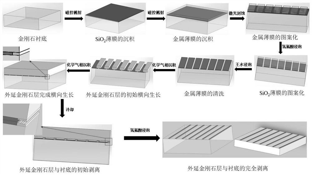
[0023] (1) Deposit a layer of 300nm thick SiO on the surface of the single crystal diamond substrate after simple polishing and cleaning with acetone and ethanol 2 thin film; (2) on SiO 2 Deposit a layer of 400nm metal Cu film on the surface of the film; (3) using laser etching method, the opening window width is 10 μm, and the mask pattern with a fill factor of 80% is transferred to a single crystal diamond substrate deposited with a metal film; ( 3) Use hydrofluoric acid solution to remove SiO at the open window 2 Thin films, SiO under metal patterns 2 The thin film is retained; (4) use aqua regia solution to remove the remaining metal thin film on the diamond substrate to obtain a patterned SiO 2 Mask the diamond substrate. (5) Using microwave plasma chemical vapor deposition method on patterned SiO 2 Homoepitaxial growth of single crystal diamond is performed on the surface of the masked diamond substrate, the microwave power of the first growth stage is controlled to ...
Embodiment 2
[0025] (1) Deposit a layer of SiO with a thickness of 400 nm on the surface of the single crystal diamond substrate after simple polishing and pretreatment with acetone and ethanol. 2 thin film; (2) on SiO 2 Deposit a layer of 500nm metal Al film on the surface of the film; (3) using laser etching method, the opening window width is 10 μm, and the mask pattern with a fill factor of 50% is transferred to a single crystal diamond substrate deposited with a metal film; ( 3) Use hydrofluoric acid solution to remove SiO at the open window 2 Thin films, SiO under metal patterns 2 The thin film is retained; (4) use aqua regia solution to remove the remaining metal thin film on the diamond substrate to obtain a patterned SiO 2 Mask the diamond substrate. (5) Using microwave plasma chemical vapor deposition method on patterned SiO 2 Homoepitaxial growth of single crystal diamond is performed on the surface of the masked diamond substrate, the microwave power of the first growth sta...
Embodiment 3
[0027] (1) Deposit a layer of SiO with a thickness of 400 nm on the surface of the single crystal diamond substrate after simple polishing and pretreatment with acetone and ethanol. 2 thin film; (2) on SiO 2 A layer of 400nm metal Ti thin film is deposited on the surface of the film; (3) using a laser etching method, the opening window width is 10 μm, and the mask pattern with a fill factor of 40% is transferred to a single crystal diamond substrate deposited with a metal thin film; ( 3) Use hydrofluoric acid solution to remove SiO at the open window 2 Thin films, SiO under metal patterns 2 The thin film is retained; (4) use aqua regia solution to remove the remaining metal thin film on the diamond substrate to obtain a patterned SiO 2Mask the diamond substrate. (5) Using microwave plasma chemical vapor deposition method on patterned SiO 2 Homoepitaxial growth of single crystal diamond is performed on the surface of the masked diamond substrate, the microwave power of the ...
PUM
| Property | Measurement | Unit |
|---|---|---|
| thickness | aaaaa | aaaaa |
| thickness | aaaaa | aaaaa |
| diameter | aaaaa | aaaaa |
Abstract
Description
Claims
Application Information
 - R&D
- Intellectual Property
- Life Sciences
- Materials
- Tech Scout
- Unparalleled Data Quality
- Higher Quality Content
- 60% Fewer Hallucinations
Browse by: Latest US Patents, China's latest patents, Technical Efficacy Thesaurus, Application Domain, Technology Topic, Popular Technical Reports.
© 2025 PatSnap. All rights reserved.Legal|Privacy policy|Modern Slavery Act Transparency Statement|Sitemap|About US| Contact US: help@patsnap.com