Capacitive differential pressure sensor, manufacturing method and application thereof

A sensor and pressure difference technology, which is applied in the field of electronic component design, can solve the problems of high process conditions and difficult process, and achieve the effect of small fixed capacitance and high resistivity

Active Publication Date: 2022-05-10
BEIHANG UNIV
View PDF11 Cites 4 Cited by
  • Summary
  • Abstract
  • Description
  • Claims
  • Application Information

AI Technical Summary

Problems solved by technology

Silicon-silicon direct bonding requires high process conditions such as bondi

Method used


Image

  • Capacitive differential pressure sensor, manufacturing method and application thereof
  • Capacitive differential pressure sensor, manufacturing method and application thereof
  • Capacitive differential pressure sensor, manufacturing method and application thereof

Examples


Embodiment 1

[0097] A device design scheme for a capacitive differential pressure sensor, including the following points:

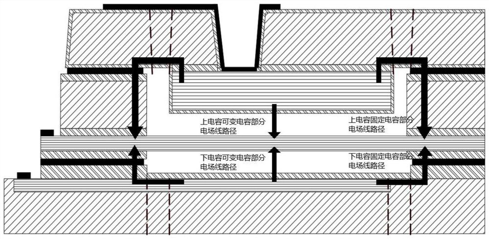
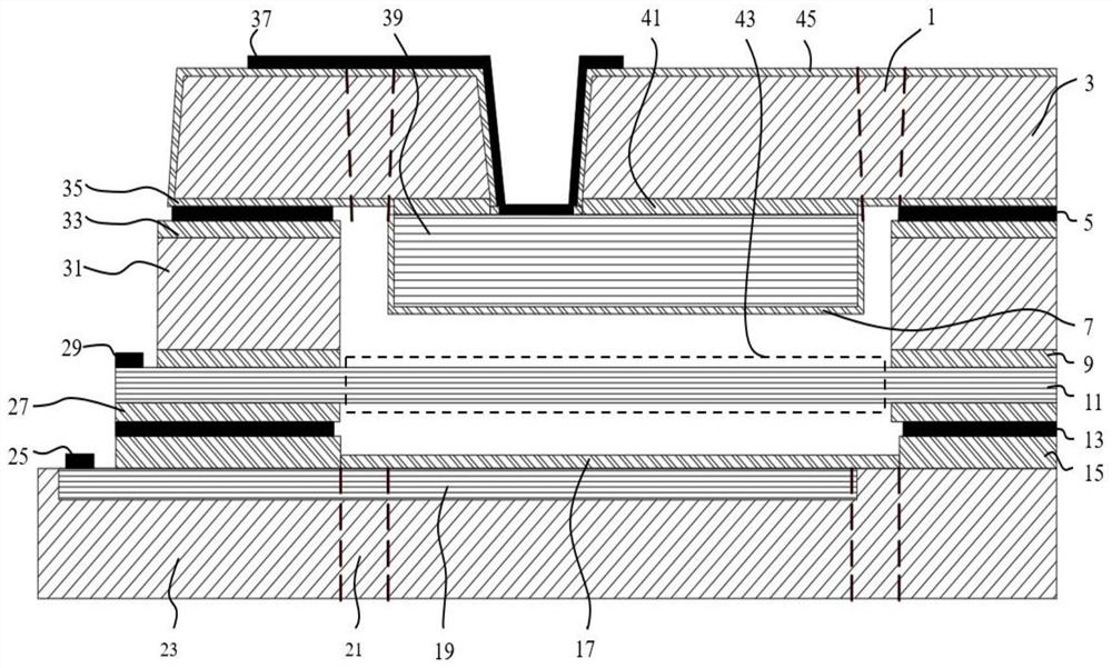
[0098] (1) The working principle of the sensor is differential capacitance, and there are three layers of electrodes on the upper, middle and lower layers, which are respectively located on the upper, middle and lower layers. The upper layer electrode 39 is located in the upper layer structure, the middle layer electrode 11 is located in the middle layer structure, and the lower layer electrode 19 is located in the lower layer structure. The middle electrode 11 forms upper and lower capacitors with the upper electrode 39 and the lower electrode 19 respectively. The pressure difference on both sides of the middle layer movable diaphragm 43 located in the middle layer electrode 11 causes the middle layer movable diaphragm 43 to deform and shift, causing the upper capacitance and lower capacitance to change, and then the signal can be output. The change of capacitance can...

Embodiment 2

[0139] MEMS (miniature electro-mechanical system) contact capacitive differential pressure sensor design method comprises the following steps:

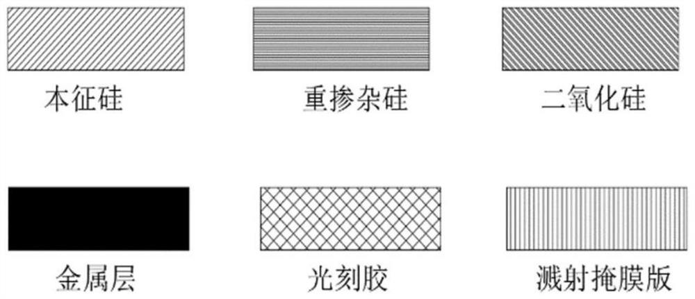
[0140] (1) For the patterned fixed electrode and its lead circuit prepared by the doping process, high-dose, high-voltage deep doping is completed on the electrode part by ion implantation. Afterwards, the wet oxidation and planarization operations on the silicon wafer are completed, and the silicon oxide layer is partially etched to expose the patterned part of the electrode. The reason for the planarization operation is that the oxidation rate of the doped part is too high, causing the oxide layer surface of the doped part to be slightly higher than that of the undoped part, and the flatness of the entire wafer exceeds the bonding requirement. .

[0141] (2) Cutting grooves are respectively etched on the upper, middle and lower bonded silicon wafers. The width of the sensor area of ​​the three silicon wafers is the same, and the le...


PUM

PropertyMeasurementUnit
Thicknessaaaaaaaaaa

Abstract

According to the differential pressure sensor, the preparation method and the application thereof, a three-layer silicon wafer bonding mode is adopted, an upper layer structure and a middle layer structure both adopt SOI wafers, and a lower layer structure adopts a graphical doped intrinsic silicon wafer; lead bonding pads of the electrodes are positioned on three steps on one side of the sensor; the peripheries of the upper electrode and the lower electrode are provided with approximately annular through holes. According to the sensor, the path of the electric field line of the fixed capacitor part is prolonged, so that the fixed capacitance in a capacitance signal output by the upper capacitor is reduced; the lower-layer structure adopts intrinsic silicon, and only the lower-layer electrode and the lead part are doped and can conduct electricity. By picking up the variable quantity of the two capacitors, the measurement of the pressure difference of fluid in the two different cavities is realized; the output sensitivity, the resolution ratio and the linearity of the sensor are all improved; external lead welding spots of the sensor are arranged at the three-layer step, an external circuit is electrically connected with a sensor lead at the three-layer step, and integration and packaging of the sensor are facilitated.

Description

technical field [0001] The invention discloses a sensor, in particular relates to a capacitive differential pressure sensor, a manufacturing method and an application thereof, and belongs to the field of electronic component design. Background technique [0002] Differential pressure sensors are used in industrial measurement technology to measure the pressure difference between two spaced chambers on a differential pressure sensor. The MEMS differential pressure sensor manufactured by MEMS technology means that it can be manufactured as a wafer composite by the known MEMS semiconductor process. [0003] Differential pressure sensors generally have an intermediate movable membrane arranged between two base bodies. In each of the two base bodies, a pressure chamber is respectively enclosed below the movable membrane of the middle layer. During the measurement operation, the cavity on one side of the movable diaphragm in the middle layer is loaded with the first pressure, an...

Claims


Application Information

Patent Timeline
IPC IPC(8): G01L13/02G01L19/06B81B7/02B81B7/00B81C1/00
CPCG01L13/026G01L19/0618B81B7/02B81B7/007B81C1/00301B81B2201/0264Y02P70/50G01L9/0073G01L9/0042G01L9/0048G01L9/12
Inventor 徐天彤李海旺曹晓达陶智翟彦欣杨春晖
Owner BEIHANG UNIV
Why Eureka
Try Eureka