
Gallium nitride nano superstructure, preparation method thereof and gallium nitride-based laser

A gallium nitride nano- and gallium nitride-based technology, which is applied in the field of gallium nitride-based lasers, gallium nitride nano-superstructure and its preparation, can solve the unfavorable development of high integration and miniaturization, and the low utilization rate of outgoing light energy , large metal absorption loss and other problems, to achieve the effect of high integration, high hardness, and low energy loss

Pending Publication Date: 2022-05-17
SUZHOU INST OF NANO TECH & NANO BIONICS CHINESE ACEDEMY OF SCI
View PDF10 Cites 2 Cited by
  • Summary
  • Abstract
  • Description
  • Claims
  • Application Information

AI Technical Summary

Problems solved by technology

[0003] The quarter-wave plate made of bulk materials is used in GaN-based blue-green lasers. Although circularly polarized light can be achieved, the overall volume is large, which is not conducive to the development of high integration and miniaturization.
The biggest problem of using metal gratings to prepare circularly polarized output lasers is that the metal has a large absorption loss, resulting in low energy utilization of the output light.

Method used


Image

  • Gallium nitride nano superstructure, preparation method thereof and gallium nitride-based laser
  • Gallium nitride nano superstructure, preparation method thereof and gallium nitride-based laser
  • Gallium nitride nano superstructure, preparation method thereof and gallium nitride-based laser

Examples


Embodiment 1

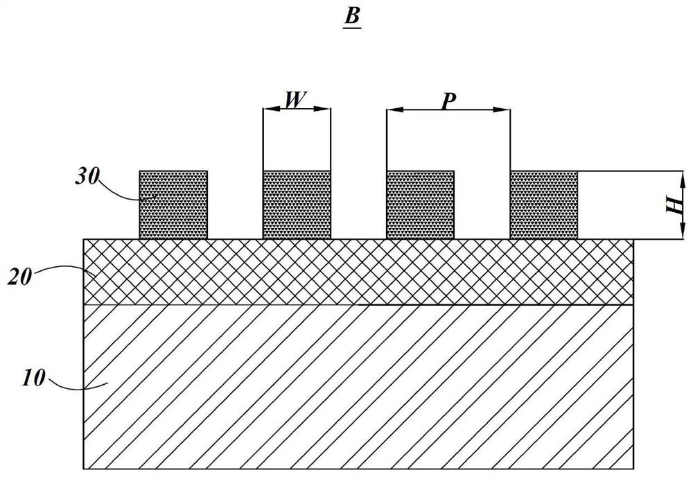
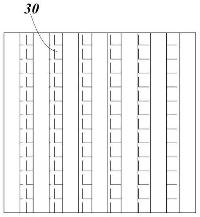
[0030] Such as figure 1 and figure 2 As shown, one embodiment of the present invention provides a gallium nitride nanosuperstructure B for integrating on a gallium nitride-based laser chip to realize circularly polarized light output from a gallium nitride-based laser. The gallium nitride nanosuperstructure is from bottom to top It includes a substrate 10 , a dielectric film layer 20 and a nano grating structure layer 30 in sequence. The size of the gallium nitride nano superstructure is 10-1000um, and the contour shape can be circular or square. The substrate 10 of the gallium nitride nano-superstructure is one of gallium nitride or sapphire. The material of the dielectric film layer 20 is one of gallium nitride, n-type gallium nitride or p-type gallium nitride, and the thickness range is 0.1um-100um. The nano-grating structure layer 30 of the gallium nitride nano-superstructure, the grating material is one of gallium nitride or n-type gallium nitride or p-type gallium ni...

Embodiment 2

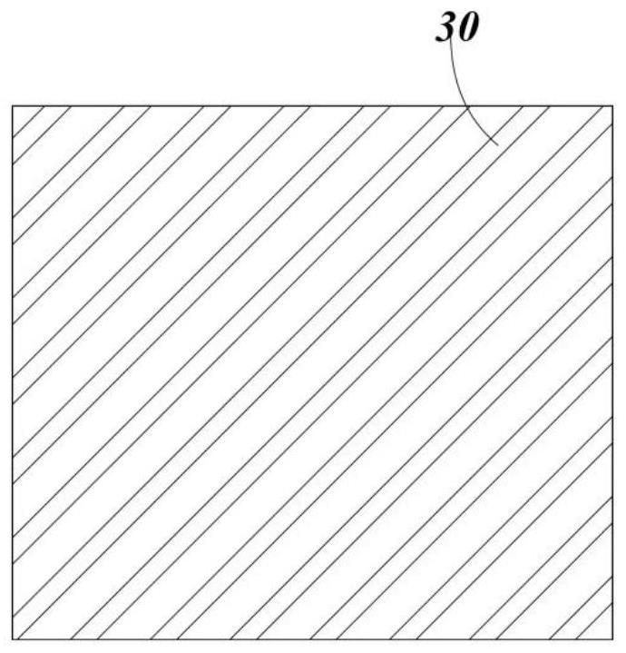
[0032] Since the above-mentioned gallium nitride nano-superstructure is used in an integrated gallium nitride-based laser, the wire grid direction of the prepared nano-grating structure layer 30 should maintain an angle of 45° with the laser chip radiation polarization direction. In order to simplify the gallium nitride The step of integrating the nano-superstructure into the gallium nitride-based laser, when the profile of the prepared gallium nitride nano-superstructure is square, a nano-grating structure with an orientation of 45° to the straight side of the substrate can be directly prepared on the dielectric film layer 20 Layer 30, Ref. image 3 shown.

[0033] refer to Figure 4As shown, the present invention also provides a method for preparing a gallium nitride nano-superstructure for realizing circularly polarized output of gallium nitride-based lasers, comprising, selecting a sapphire substrate, growing gallium nitride or n-type gallium nitride or p-type gallium ni...

Embodiment 3

[0036] Firstly, the GaN thin film grown on the sapphire substrate 10 or the GaN single crystal substrate is directly spin-coated with 200 nm of photoresist. A grating pattern with a period of 220nm and a width of 140nm is exposed by electron beam lithography or double-beam ultraviolet exposure, and developed. Electron beam evaporation or magnetron sputtering is used to vapor-deposit metal chromium with a thickness of 50 nm on the above-mentioned structure, and the photoresist structure is removed by ultrasonic soaking in acetone. At this time, the width of the metal chromium grating is 80 nm. The gallium nitride is etched by dry etching (ICP) to a depth of 225nm and a width of 80nm, and residual chromium is washed away using a chromium etching solution. The transmittance lines and the phase difference and amplitude of the prepared gallium nitride supernanostructures in the blue light broad spectrum band, such as Figure 5a and Figure 5b shown.


PUM

PropertyMeasurementUnit
heightaaaaaaaaaa
thicknessaaaaaaaaaa
depthaaaaaaaaaa

Abstract

The invention discloses a gallium nitride nano superstructure, a preparation method thereof and a gallium nitride-based laser with the gallium nitride nano superstructure. The gallium nitride nano superstructure is used for realizing circular polarization light emission of the gallium nitride-based laser. The gallium nitride nano superstructure sequentially comprises a substrate, a dielectric film layer and a nano grating structure layer from bottom to top, a grating material of the nano grating structure layer comprises one of gallium nitride, n-type gallium nitride and p-type gallium nitride, the grating period range is 100 nm to 280 nm, the grating height range is 100 nm to 300 nm, and the grating line width is 50 nm to 200 nm. The gallium nitride nano superstructure can realize an efficient circular polarization light emitting function, and circular polarization light emitting of a gallium nitride-based laser can be realized when the gallium nitride nano superstructure is applied to the gallium nitride-based laser.

Description

technical field [0001] The invention relates to the technical field of micro-nano manufacturing, in particular to a gallium nitride nano-superstructure for realizing circularly polarized output of a gallium nitride-based laser, a preparation method thereof, and a gallium nitride-based laser. Background technique [0002] Gallium nitride-based blue-green lasers have achieved important applications in the fields of laser display, laser projection, and visible light communication due to their advantages such as high luminous efficiency, narrow linewidth, and high color rendering index. If it is further used in holographic display, biological imaging, underwater optical communication, quantum communication and other fields, it is necessary to convert the GaN-based laser that is linearly polarized light by adding specific optical elements (such as a quarter-wave plate) Radiation with circularly polarized light. Generally, the quarter-wave band used to obtain circularly polarized...

Claims


Application Information

Patent Timeline
Patent Type & Authority Applications(China)
IPC IPC(8): G02B5/30G02B1/00H01S5/00
CPCG02B5/3058G02B1/002H01S5/0085G02B5/1809Y02P70/50H01S5/32341H01S5/18386H01S5/005B82Y20/00H01S5/0213H01S5/1082H01S5/02257H01S5/02469H01S2301/14G03F7/0005H01S5/323
Inventor 王淼易觉民王建峰徐科
Owner SUZHOU INST OF NANO TECH & NANO BIONICS CHINESE ACEDEMY OF SCI
Learn More