Electron selective passivation contact structure, solar cell and preparation method

A technology of electron selectivity and solar cells, which is applied in the field of solar cells, can solve the problems of poor passivation contact performance, large near-infrared absorption loss, and poor passivation contact performance, so as to achieve low carrier recombination rate and improve photoelectricity. Transformation efficiency, low cost effect

Active Publication Date: 2022-06-28
SUZHOU UNIV
View PDF7 Cites 1 Cited by
  • Summary
  • Abstract
  • Description
  • Claims
  • Application Information

AI Technical Summary

Problems solved by technology

However, up to now, only a-Si:H / MoOx / ITO hole-selective passivation contacts have been successfully applied to the front end of SHJ batteries, and some progress has been made, but the thermal stability of this structure is relatively low. Poor, the passivation contact performance needs to be improved; while the electronically selective passivation contacts developed are all used on the back end of crystalline silicon cells, and usually only a few nanometers are stacked with metal electrodes, due to the near-infrared absorption loss caused by the excitation of surface plasmon elements Larger; a few reported highly transparent electronically selective passivation contacts, such as a-Si:H / TiO2 / ITO, have poor passivation contact performance (especially large contact resistance), Device conversion efficiency is very low

Method used


Image

  • Electron selective passivation contact structure, solar cell and preparation method
  • Electron selective passivation contact structure, solar cell and preparation method
  • Electron selective passivation contact structure, solar cell and preparation method

Examples


Embodiment 1

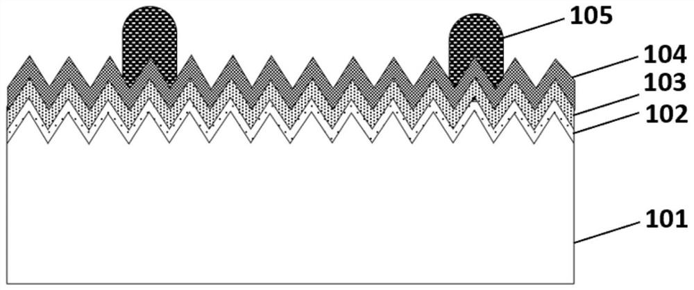
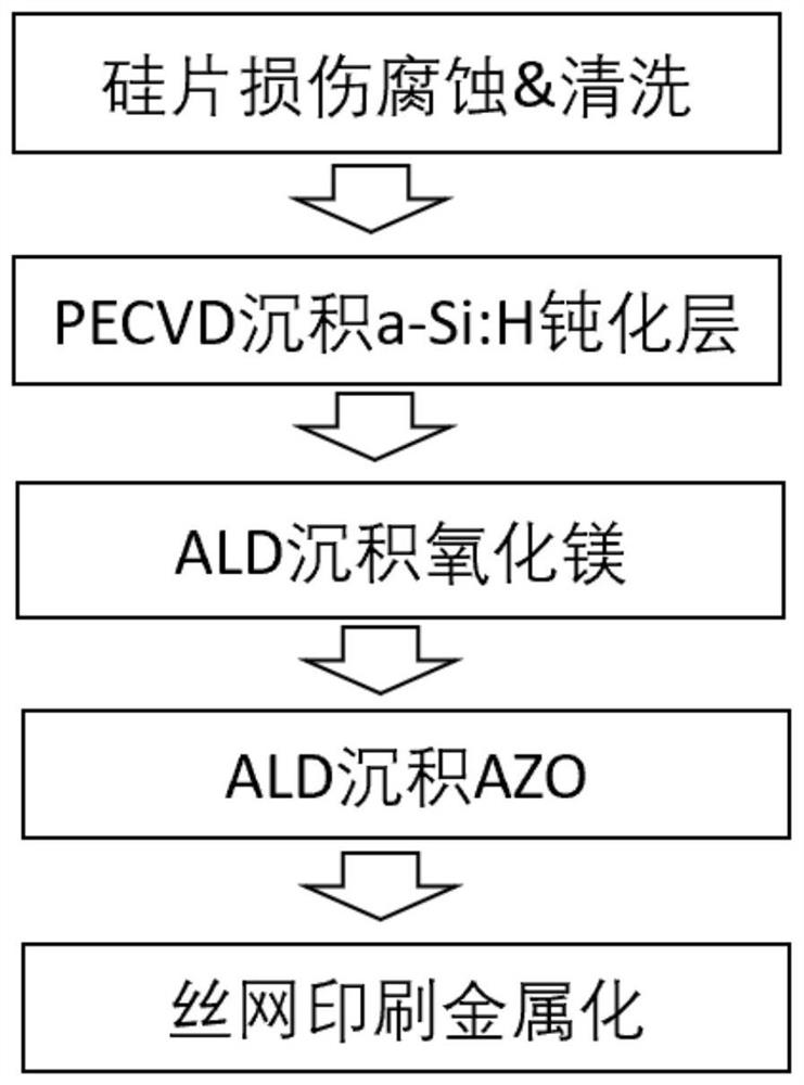
[0064] This embodiment provides a method for realizing electron selective passivation contact structure, and its structure and preparation process flow chart are respectively as follows figure 1 and figure 2 It mainly includes the following steps:

[0065] 1) select a kind of n-type single crystal silicon wafer, use potassium hydroxide KOH alkali solution to carry out polishing etching to remove the damaged layer and make texturing, then RCA cleaning to obtain silicon substrate 101;

[0066] 2) Using plasma enhanced chemical vapor deposition (PECVD) technology to deposit hydrogenated amorphous silicon (a-Si:H) tunneling passivation layer 102 on the surface of the silicon wafer, the thickness of the a-Si:H passivation layer is 5nm, and the deposition temperature is 200°C ;

[0067] 3) A magnesium oxide (MgO) film 103 is deposited on the a-Si:H passivation layer, prepared by atomic layer deposition (ALD), and the thickness is 3.0 nm;

[0068] 4) Aluminium-doped zinc oxide (A...

Embodiment 2

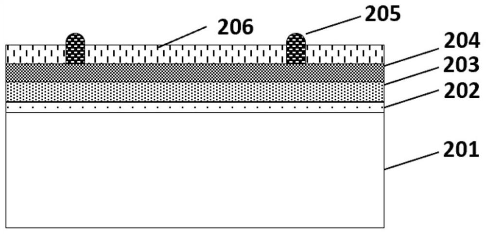
[0072] This embodiment provides a method for realizing an electron selective passivation contact structure based on Embodiment 1. The main feature is that an anti-reflection film is superimposed on the thinned ZnO transparent electrode to further reduce parasitic absorption and reflectivity. And the preparation process flow chart are as follows image 3 and Figure 4 As shown, it mainly includes the following process steps:

[0073] 1) select a kind of p-type single crystal silicon wafer, carry out polishing and etching with potassium hydroxide KOH alkali solution to remove the damaged layer, then RCA cleans to obtain silicon substrate 201;

[0074] 2) using PECVD to deposit a-Si:H tunneling passivation layer 202 on the surface of the silicon wafer, the thickness of the a-Si:H passivation layer is 5nm, and the deposition temperature is 200°C;

[0075] 3) ALD method is used to deposit MgO thin film 203 on the a-Si:H passivation layer with a thickness of 3.0 nm and a depositio...

Embodiment 3

[0081] This embodiment provides a method for realizing electron-selective passivation contact structure based on Embodiment 2, the main feature is that the tunneling silicon oxide (SiO 2 ) The passivation layer replaces the a-Si:H passivation layer and has higher transparency. Its structure and preparation process flow chart are as follows Figure 5 and Image 6 As shown, it mainly includes the following process steps:

[0082] 1) select a kind of n-type single crystal silicon wafer, use potassium hydroxide KOH alkali solution to carry out polishing and etching to remove the damaged layer, then RCA cleaning to obtain silicon substrate 301;

[0083] 2) Using ALD method to deposit tunnel SiO on the surface of silicon wafer 2 The passivation layer 302 has a thickness of about 1.5nm and a deposition temperature of 200°C;

[0084] 3) In SiO 2 ALD method is used to deposit MgO film 303 on the passivation layer, the thickness is 4.0nm, and the deposition temperature is 200℃;

[...


PUM

PropertyMeasurementUnit
thicknessaaaaaaaaaa
thicknessaaaaaaaaaa
thicknessaaaaaaaaaa

Abstract

The invention discloses an electron selective passivation contact structure, a solar cell and a preparation method. The electron selective passivation contact structure comprises a crystalline silicon substrate; the tunneling passivation layer is deposited on the crystalline silicon substrate; the electron transport layer is deposited on the tunneling passivation layer, and the electron transport layer is a magnesium oxide film; the transparent electrode is deposited on the electron transport layer, and the transparent electrode is a zinc oxide transparent electrode; and the metal electrode is deposited on the zinc oxide transparent electrode. The crystalline silicon solar cell has high transparency and excellent passivation contact performance, carrier recombination loss at the metal-crystalline silicon contact position can be effectively reduced, parasitic optical absorption can be reduced, and the photoelectric conversion efficiency of the crystalline silicon solar cell is improved.

Description

technical field [0001] The invention relates to the technical field of solar cells, in particular to an electron selective passivation contact structure, a solar cell and a preparation method. Background technique [0002] The main theme of the development of solar photovoltaic technology is to improve the conversion efficiency and reduce the manufacturing cost, thereby reducing the cost of electricity (LCOE). At present, the mainstream products in the market are PERC cells (Passivated Emitter and Rear Cell) based on high temperature doped homojunction, whose conversion efficiency limit is about 24%, which is mainly limited by the high carrier recombination loss at the crystalline silicon-electrode contact interface. , as well as Auger recombination, band gap narrowing and free carrier absorption induced by heavy doping. Therefore, reducing the carrier recombination loss at the crystalline silicon-electrode contact interface and reducing or removing the doping process are t...

Claims


Application Information

Patent Timeline
Patent Type & Authority Applications(China)
IPC IPC(8): H01L31/0224H01L31/0216H01L31/06H01L31/18
CPCH01L31/022466H01L31/02168H01L31/06H01L31/1868H01L31/1804Y02E10/50Y02P70/50
Inventor 杨新波
Owner SUZHOU UNIV
Why Eureka
Try Eureka