Photoelectronic device and its producing method and electronic device with said photoelectronic device

An electro-optical device and a manufacturing method technology, which are applied to identification devices, cathode ray tubes/electron beam tubes, devices for coating liquid on surfaces, etc. bumpy effect

Inactive Publication Date: 2005-05-18
SEIKO EPSON CORP
View PDF6 Cites 3 Cited by
  • Summary
  • Abstract
  • Description
  • Claims
  • Application Information

AI Technical Summary

Problems solved by technology

[0012] In addition, when there are finally steps on the surface of the substrate, for example, in a liquid crystal device, the alignment treatment of the alignment film that limits the alignment direction of the electro-optic material cannot be sufficiently performed on the step portion, resulting in display quality such as a local decrease in contrast. Lowering the problem
[0013] In addition, in a liquid crystal device or the like, since it is generally intended to be driven by an electric field perpendicular to the substrate (hereinafter referred to as "longitudinal electric field"), when an electric field along the direction of the substrate (hereinafter referred to as "longitudinal electric field") is generated near the end of the pixel electrode is "horizontal electric field"), the display quality will be degraded
Especially when the surface of the TFT array substrate is uniformly planarized as described above, there will be a problem that the adverse effect of the lateral electric field will be strengthened instead.

Method used


Image

  • Photoelectronic device and its producing method and electronic device with said photoelectronic device
  • Photoelectronic device and its producing method and electronic device with said photoelectronic device
  • Photoelectronic device and its producing method and electronic device with said photoelectronic device

Examples


Embodiment 1

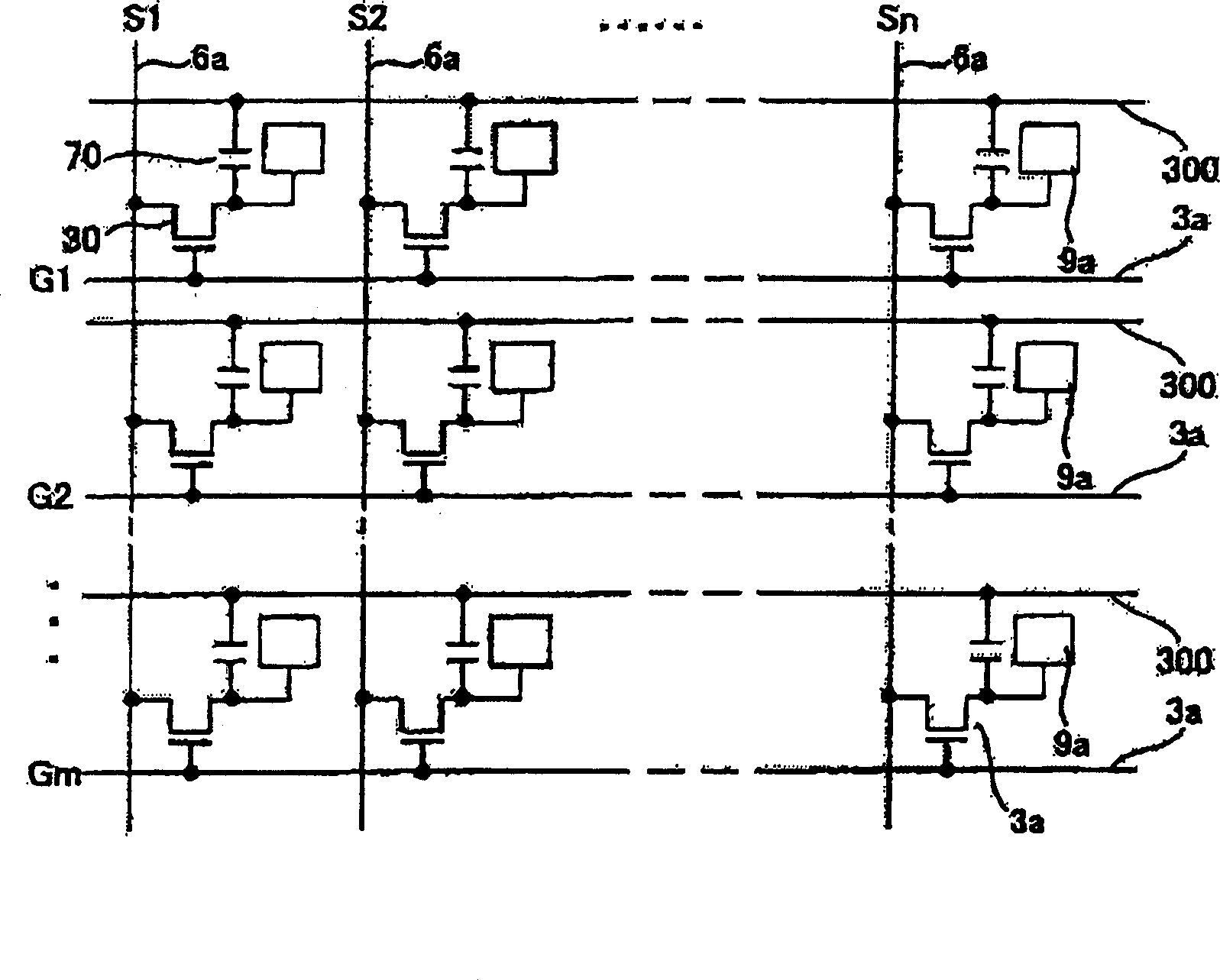
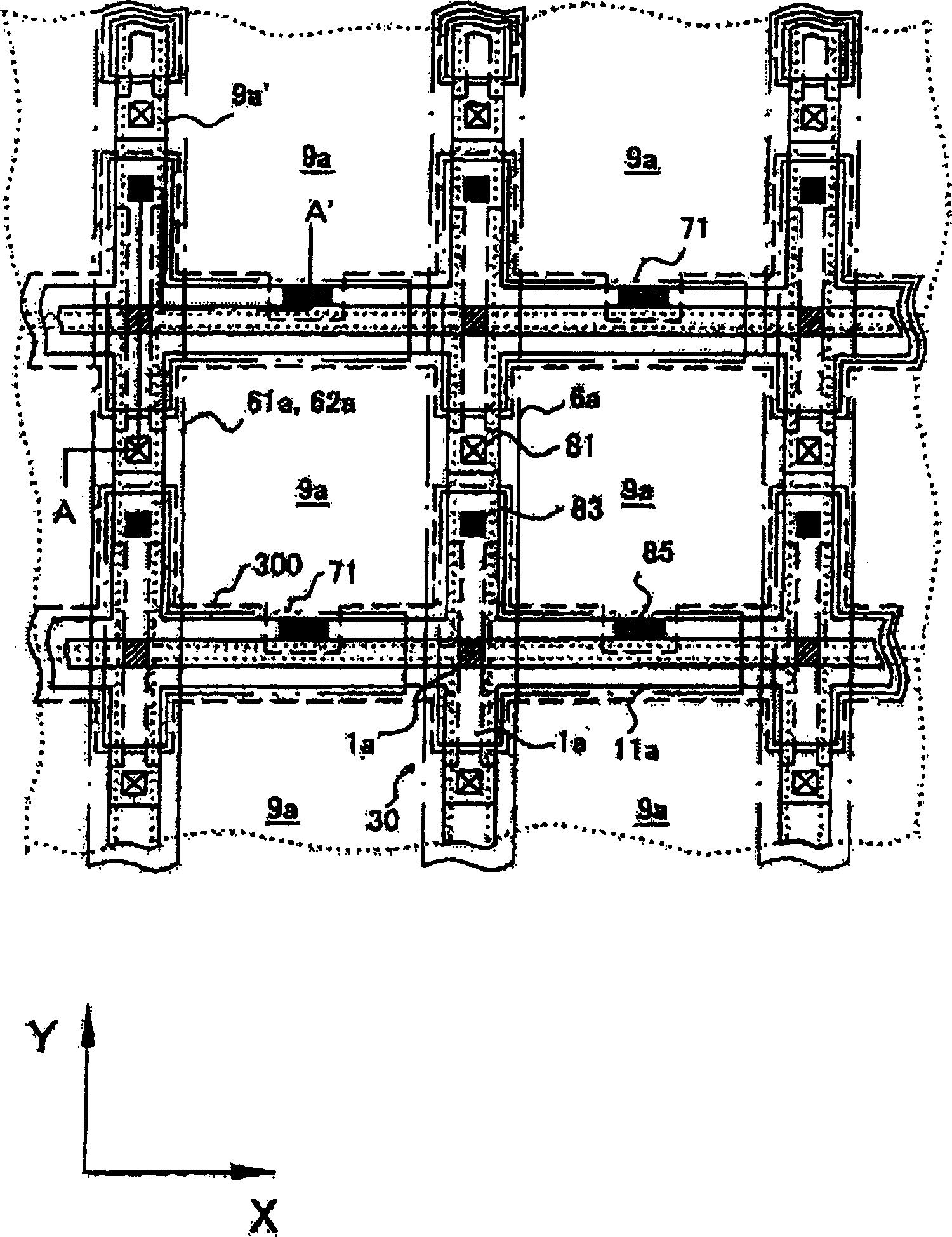
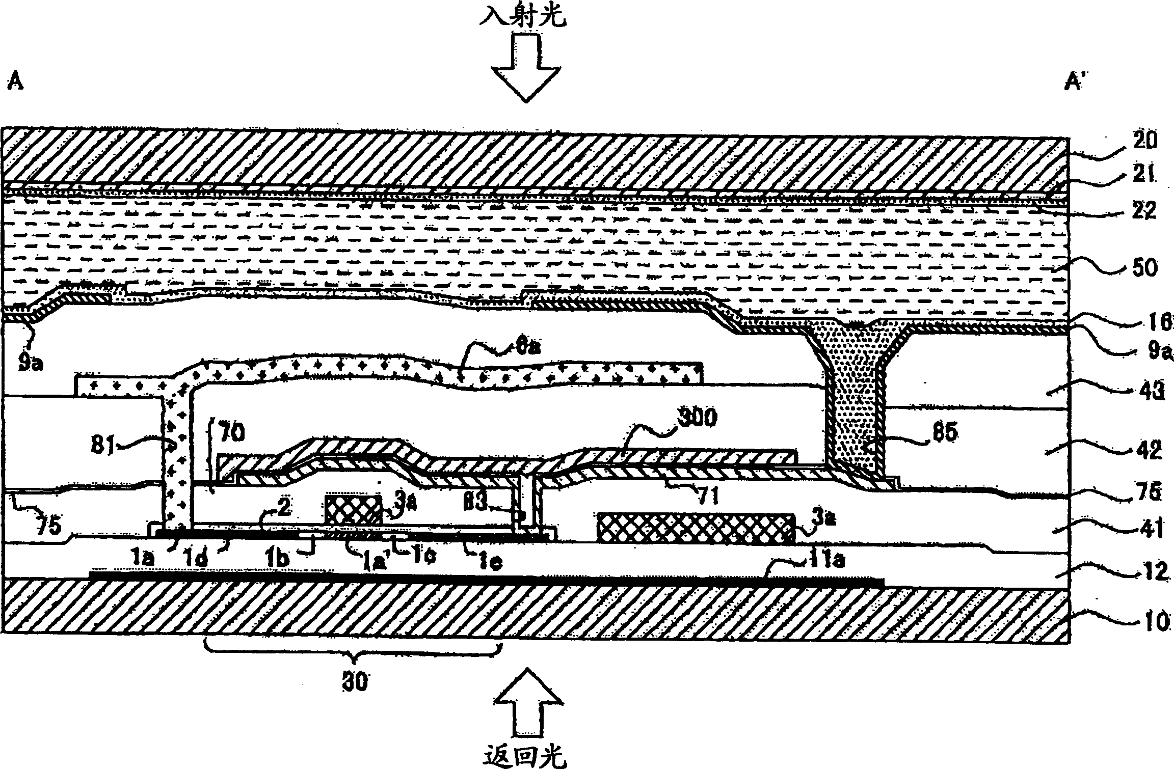
[0146] The electro-optical device was produced in the same manner as in the above-mentioned embodiment. At this time, as shown in FIG. 10, a pattern 61 is formed on the quartz substrate, and a BPSG film 62 with a film thickness of 800 nm is formed on the entire surface. The pattern 61 corresponds to the scanning line 3a of the embodiment, and the BPSG film 62 corresponds to the first interlayer insulating film 41 of the embodiment. Next, the substrate is heat-treated at a temperature of 890° C., and the BPSG film 61 is reflowed and planarized. After the processing, the inclination angle of the step portion of the BPSG film 62 generated by the pattern 61 is measured as the reflow angle θ.

[0147] The concentration of boron (B) in the BPSG film 62 was changed from 0.8% by weight to 5% by weight, and the above-mentioned measurement was performed for each case. In addition, the concentration of phosphorus (P) is all 6 wt%.

[0148] The measurement results obtained in this way are as ...

Embodiment 2

[0151] An electro-optical device was produced in the same manner as in Example 1. However, when the BPSG film 62 is formed on the quartz substrate on which the pattern 61 is formed, in this embodiment, the concentration of boron in the BPSG film 62 is fixed at 3% by weight, and the concentration of phosphorus (P) is fixed at 6% by weight. On this basis, the heating temperature (reflow temperature) was changed to 850°C, 900°C, and 950°C for flattening, and the reflow angle θ was measured for various situations.

[0152] The measurement results obtained in this way are as Picture 12 Shown. Picture 12 It represents the change of the reflow angle θ with respect to the reflow temperature of the BPSG film 62. When the reflow temperature is about 850°C, the reflow angle θ is about 86°, and the step is still steep. However, when the reflow temperature is about 900°C, the reflow angle θ is about 45°, and it can be seen that the step has become gentle. Furthermore, when the reflow tempera...

Embodiment 3

[0155] Below, Table 1 shows the precipitation status of phosphorus and boron. The amount of phosphorus and boron can be changed to form a BPSG film, and the precipitation of phosphorus and boron can be detected visually. In addition, the flow rate of ozone during the formation of the BPSG film was kept constant (80 slm) in all samples.

[0156] P(wt%)

[0157] As shown in Table 1, in the BPSG film in which the total weight% of phosphorus and boron is 11% by weight, the precipitation of phosphorus or boron was confirmed within one day after the film formation. In addition, the inventors of the present application can confirm that as the total weight% of phosphorus and boron decreases, the time until the precipitation of phosphorus or boron gradually increases. In addition, under the condition that the total weight% of phosphorus and boron is less than or equal to 10% by weight, it takes 2 days or more than 2 days until phosphorus or boron is precipitated. Therefore, it ca...


PUM


Abstract

The present invention provides electro-optical devices that can be manufactured with high yield and display high quality. In this electro-optical device, the substrate has electrodes for display, at least one of wirings for driving the electrodes for display, and electronic components, and at least one of the electrodes for display, wirings, and electronic components for electrically connecting each other with each other. An interlayer insulating film provided on the lower layer of the display electrode for insulation. At least one of the interlayer insulating films is composed of a borophosphosilicate glass film and has been subjected to a planarization process in a fluidized state.

Description

Technical field [0001] The present invention relates to a method for manufacturing an electro-optical device such as a liquid crystal device, the electro-optical device, and electronic equipment such as a liquid crystal projector. Background technique [0002] In this type of electro-optical device, the display electrodes, the scanning lines, data lines, and other wiring and electronic components that drive the electrodes are stacked on a substrate with an interlayer insulating film interposed therebetween. When the electro-optical device adopts the active matrix driving method, a thin film transistor (ThinFilm Transistor: hereinafter referred to as "TFT") for pixel switching is formed on the substrate. Among them, in the high-temperature process type polysilicon TFT, the formation of the thermally oxidized gate insulating film requires a heat treatment of 1000° C. or more. Therefore, the interlayer insulating film basically requires heat resistance. For example, it is preferable...

Claims


Application Information

Patent Timeline
Patent Type & Authority Applications(China)
IPC IPC(8): G02F1/1368B05D5/06B05D5/12G02F1/133G02F1/1333G02F1/136G02F1/1362G09F9/30G09G3/36H01J29/00H01L21/00H01L21/316H01L21/336H01L29/786
CPCG02F1/136227G02F1/1333
Inventor 福原圭司森肋稔
Owner SEIKO EPSON CORP
Why Eureka
Try Eureka