Thin film multilayer body, electronic device using such thin film multilayer body, actuator, and method for manufacturing actuator

A technology of laminates and regulators, applied in the manufacture/assembly of piezoelectric/electrostrictive devices, semiconductor/solid-state device manufacturing, chemical instruments and methods, etc., can solve the problems of piezoelectricity or electrostriction degradation, Problems such as crystallographic orientation change and polarization direction deviation, etc., to achieve the effect of excellent crystallinity, good crystallinity, and good polarization amount

Inactive Publication Date: 2005-11-02
FUJITSU LTD
View PDF1 Cites 5 Cited by
  • Summary
  • Abstract
  • Description
  • Claims
  • Application Information

AI Technical Summary

Problems solved by technology

[0010] However, when a conductive layer is provided, if the conductive layer has low crystallinity, or cannot epitaxially grow on the magnesium aluminate spinel film, there may be low crystallinity or calcium formed on the conductive layer. Changes in the crystallographic orientation of the titanium oxide layer, severe deviation from the polarization direction, and deterioration of piezoelectricity or electrostriction

Method used


Image

  • Thin film multilayer body, electronic device using such thin film multilayer body, actuator, and method for manufacturing actuator
  • Thin film multilayer body, electronic device using such thin film multilayer body, actuator, and method for manufacturing actuator
  • Thin film multilayer body, electronic device using such thin film multilayer body, actuator, and method for manufacturing actuator

Examples


no. 1 Embodiment approach

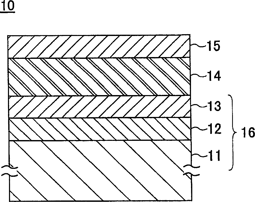
[0054] figure 1 It is a cross-sectional view of the regulator according to the first embodiment of the present invention.

[0055] refer to figure 1 The regulator 10 of this embodiment has a structure in which an intermediate layer 12 , a lower conductive layer 13 , an oxide layer 14 , and an upper conductive layer 15 are sequentially stacked on a single crystal substrate 11 . The regulator 10 is stretched longitudinally by applying a voltage between the lower conductive layer 13 and the upper conductive layer 15 , utilizing the piezoelectricity and electrostriction of the oxide layer 14 , for example, utilizing the longitudinal effect of the oxide layer 14 .

[0056] The single crystal substrate 11 is, for example, a silicon or gallium-arsenic (GaAs) single crystal substrate. The thickness of the single crystal substrate 11 is about 500 μm, and the main surface is a (001) plane. By setting the principal plane as (001), the plane orientations of the layers epitaxially grown...

no. 1 Embodiment

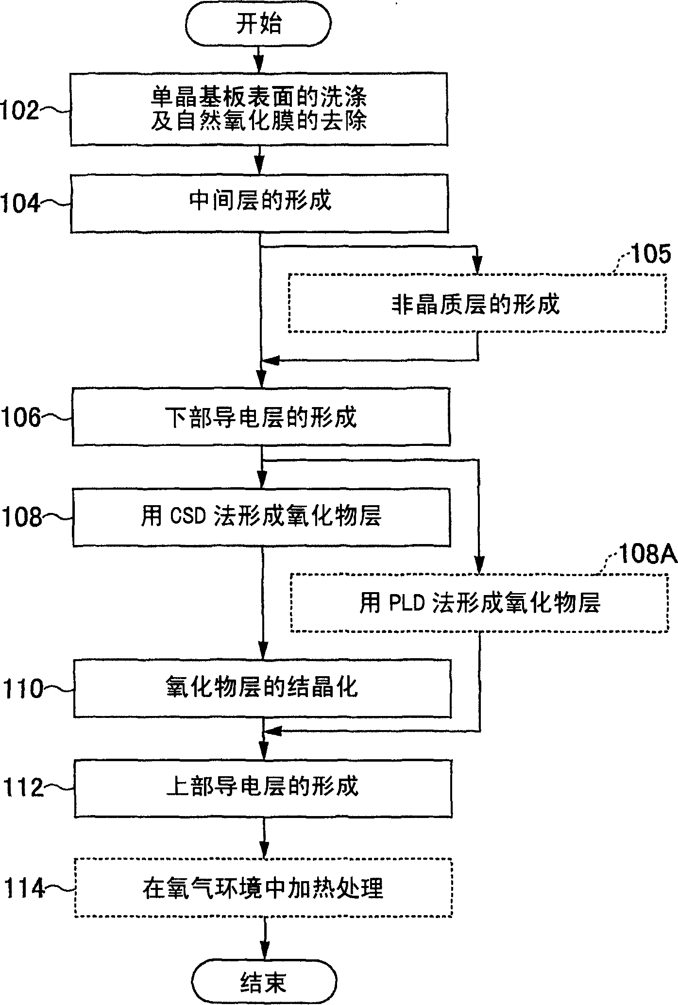
[0087] Hereinafter, a regulator according to an example of the present embodiment will be described. The regulator of this embodiment is formed by sequentially laminating a platinum film as a lower conductive layer (electrode), a PZT film as an oxide layer, and an upper conductive layer on a silicon single crystal substrate.

[0088] First, after washing the 2-inch silicon single crystal substrate with the (001) plane as the main surface, it is immersed in 9% by mass of dilute hydrofluoric acid to remove the natural oxide film (SiO2) of the single silicon crystal substrate. 2 ).

[0089] Then, magnesium aluminate spinel with a thickness of 100 nm was formed on the silicon single crystal substrate by the CVD method. Specifically, the silicon single crystal substrate is placed in a CVD film forming chamber and kept at a substrate temperature of 900°C. Mg raw material adopts MgCl 2 , heated to 500°C in the Mg source chamber to make it evaporate, and the carrier gas is hydrogen...

no. 2 Embodiment

[0096] The regulator of this embodiment is the same as that of the first embodiment except that an iridium film is formed instead of the platinum film of the lower conductive layer of the first embodiment, and PLZT is used for the oxide layer. The description of the same manufacturing process as that of the first embodiment is omitted.

[0097] The regulator of this example is formed by sequentially laminating magnesium aluminate spinel, an iridium film as a lower conductive layer, a PLZT film as an oxide layer, and an upper conductive layer on a silicon single crystal substrate.

[0098] The iridium film was formed to a thickness of 200 nm on the magnesium aluminate spinel film by sputtering. Specifically, make the inside of the sputtering device reach 1Pa (7.5×10 -3 Torr) while flowing 30 sccm of argon gas and 1 sccm of oxygen gas, the substrate was heated to 600° C. for epitaxial growth.

[0099] The PLZT film is formed on the iridium film by the CSD method. Specifically...


PUM

PropertyMeasurementUnit
thicknessaaaaaaaaaa
thicknessaaaaaaaaaa

Abstract

An actuator (10) is formed by sequentially stacking an intermediate layer (12), a lower conductive layer (13), an oxide layer (14), and an upper conductive layer (15) on a silicon or GaAs single crystal substrate (11). The intermediate layer (12) of magnesia spinel (MgAl2O4), the lower conductive layer (13) of a platinum-group element or its alloy, and the oxide layer (14) of a crystalline structure having a simple perovskite lattice are epitaxially grown and formed. The oxide layer (14) is composed of a crystal having a simple perovskite lattice, and its (001) surface grows epitaxially. Accordingly, the oxide layer (14) has good crystallinity, and is excellent in dielectric constant, piezoelectric property, and electrostrictive property since a voltage application direction matches the polarization axis.

Description

technical field [0001] The present invention relates to a thin film laminate capable of epitaxially growing an oxide layer having a crystal structure of a simple perovskite lattice in a crystal exhibiting high dielectric properties, piezoelectricity, dielectric properties, pyroelectricity, etc., and forming A thin film laminate having the oxide layer, and an electronic device having the thin film laminate having the oxide layer formed thereon. The electronic device is suitably used for, for example, a driver for a precision positioning regulator, a buzzer, or the like, a capacitor element, a DRAM, FeRAM, a SAW device, and the like. Background technique [0002] In recent years, there has been a strong desire for small and high-performance actuators that can be used in various drive devices, such as head positioning mechanisms for magnetic disk devices or drive mechanisms for medical micromachines. For regulators that must be miniaturized in this way, a piezoelectric materia...

Claims


Application Information

Patent Timeline
Patent Type & Authority Applications(China)
IPC IPC(8): C30B29/26C23C16/40G02F1/1339H01L21/8246H01L27/105H01L41/08H01L41/09H01L41/18H01L41/187H01L41/22H01L41/29H01L41/317H01L41/39
CPCH01L41/0815H01L41/319H01L41/1875H01L41/29H01L41/257H10N30/10516H10N30/8548H10N30/079H10N30/06H10N30/00
Inventor 近藤正雄山胁秀树
Owner FUJITSU LTD
Why Eureka
Try Eureka