Process for preparing nitrigen-aluminium co-blended hole zinc oxide thin film material

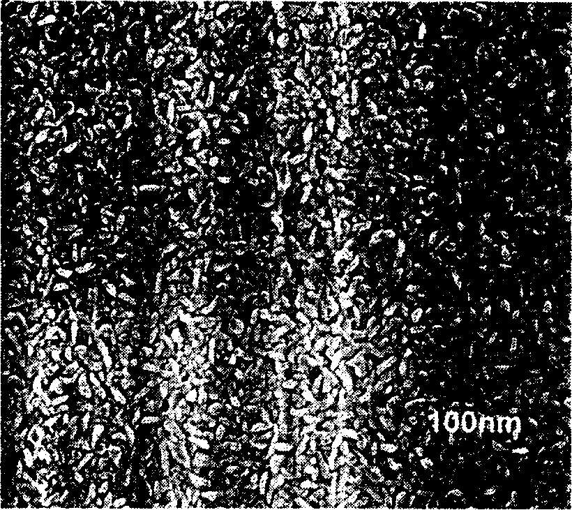
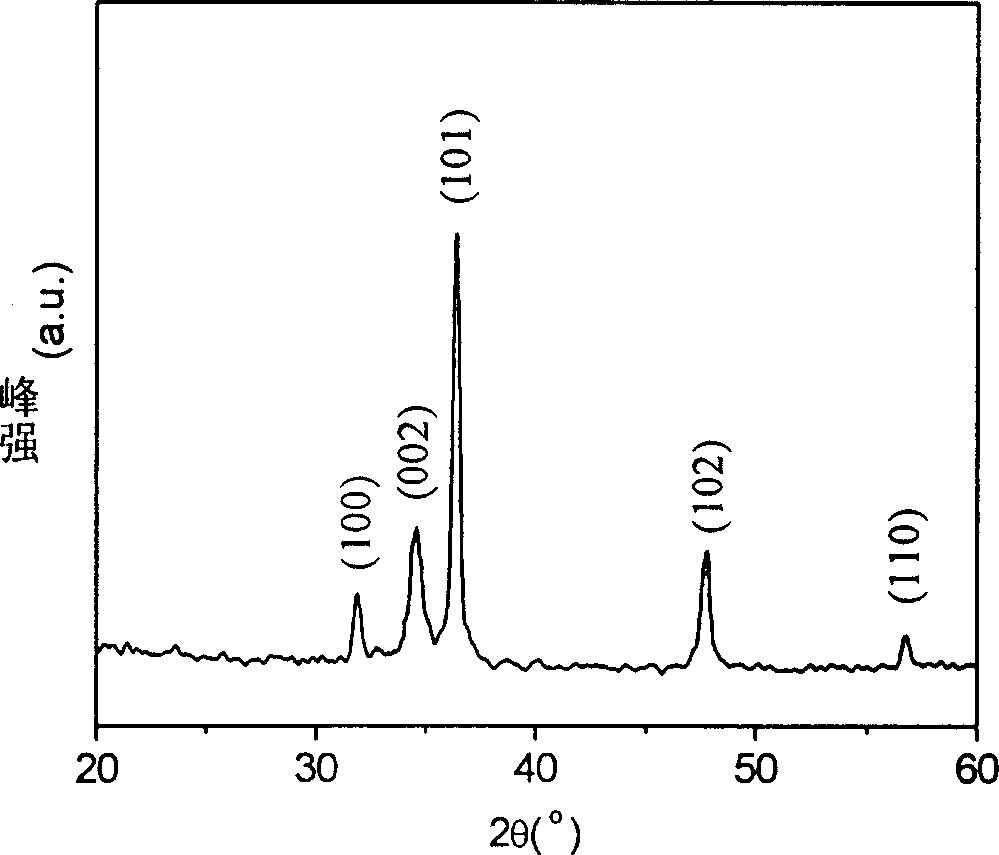
A zinc oxide thin film and preparation process technology, applied in semiconductor/solid-state device manufacturing, laser parts, semiconductor lasers, etc., can solve the problems of low carrier mobility, difficulty, enhanced self-compensation effect, etc., and achieve strong room temperature ultraviolet Effects of luminescent properties, uniform grain size, and strong crystalline properties

Inactive Publication Date: 2006-06-07
SHANGHAI INST OF CERAMIC CHEM & TECH CHINESE ACAD OF SCI
View PDF0 Cites 7 Cited by
  • Summary
  • Abstract
  • Description
  • Claims
  • Application Information

AI Technical Summary

Problems solved by technology

The active N source in the first type generally comes from N 2 , N 2 O or NH 3 , but when N replaces O atoms, the Madelung Energy is increased, which causes the localization of the N energy level, the N energy level is deep, and the doping effect is not very ideal.
The second and third types need to use higher-priced Ga and In sources, and the production cost is high.
[0004] At present, the preparation of p-type ZnO thin films mostly adopts magnetron sputtering and pulsed laser deposition (PLD) technology, but it is quite difficult to obtain p-type ZnO thin films with low resistance and high mobility.
For example, Ohshima et al. from Kumamoto University in Japan have used the N + or N 2 + Ion-sputtered Al mesh electrodes to perform N-Al co-doping on undoped ZnO thin films deposited by KrF excimer pulse laser (T. Ohshima et al., Thin Solid Films, 435, 49 (2003)), but the result Have not obtained p-type ZnO thin film; The p-type ZnO thin film obtained by N-Al co-doping (Ye Zhizhen et al., Journal of Crystal Growth 265,127 (2004)) to ZnO by DC reactive magnetron sputtering method, Its resistivity is 10 2 -10 4 Ωcm, the mobility is 0.3-19cm 2 V -1 the s -1 ; The higher level of p-type ZnO film developed by the above-mentioned Japanese Kawawa laboratory with the PLD method has a high resistivity and a low carrier mobility, which cannot meet the practical requirements
The reason is that these two methods require high vacuum conditions, so the resulting ZnO film has a high concentration of oxygen vacancies, which makes the self-compensation effect in the film significantly enhanced, and the concentration of N acceptors is very low, so it is necessary to make N provide It is very difficult to obtain enough hole carriers for p-type conduction in ZnO
In addition, magnetron sputtering and PLD equipment are expensive, the cost of film production is high, and it is difficult to achieve large-area deposition

Method used


Image

  • Process for preparing nitrigen-aluminium co-blended hole zinc oxide thin film material
  • Process for preparing nitrigen-aluminium co-blended hole zinc oxide thin film material
  • Process for preparing nitrigen-aluminium co-blended hole zinc oxide thin film material

Examples


Embodiment 1

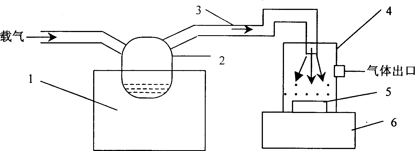
[0037] The substrate is a (100) plane single crystal silicon wafer. The ratio of the precursor solution is: 1M Zn(CH 3 COO) 2 5mL, 5M CH 3 COONH 4 3mL, 0.5M Al(NO 3 ) 3 0.5mL. The solvent used was deionized water. Pour the prepared precursor solution into the ultrasonic atomization cup. After the single crystal (100) silicon wafer was etched with hydrofluoric acid for 3 minutes, it was immediately fixed on the furnace plate, and the furnace plate was heated to 700 ° C. After the substrate reached the set temperature, the ultrasonic atomizer was started to Pure N 2 (99.999%) as the carrier gas, while the film-forming chamber maintains an atmospheric atmosphere. The atomized gas enters the film-forming chamber through the gas-liquid separation tube, and the distance between the nozzle and the substrate is kept at about 5 cm, and the spraying is stopped for about 10 minutes. Precursor solution consumption rate is O.2ml / cm 2 min. After incubation at 700°C for 5 minutes,...

Embodiment 2

[0040] The ratio of the precursor solution is: 1M Zn(CH 3 COO) 2 5mL, 5M CH 3 COONH 4 2mL, 0.5M AlCl 3 0.5mL. The substrate temperature was 650°C. The spray time is 6 minutes. After the deposition of the thin film, it was kept at 650° C. for 5 minutes and then lowered to room temperature. Other conditions are the same as Example 1. The Hall effect test of the grown ZnO thin film shows that the conductivity type is p-type, that is, hole conduction. Resistivity 1.6×10 -2 Ωcm, carrier mobility 103cm 2 V -1 the s -1 , carrier concentration 3.81×10 18 cm -3 .


PUM


Abstract

This invention relates to a NAL common doped cavity ZnO film and a preparing technology, which applies the supersonic spray pyrogenation method and takes the mixed solution of the organic or inorganic solution of Zn, the organic or inorganic solution of N and the inorganic solution of Al as the precursor to control the electric performance of type-P ZnO film by regulating and controlling the substrate temperature at 600-900deg.C, the movability can reach to 103cm at the maximum.

Description

technical field [0001] The invention relates to a preparation process of a nitrogen-aluminum co-doped hole-type zinc oxide film material used for zinc oxide-based light-emitting diodes (LEDs), laser diodes (LDs) and ultraviolet detectors and other optoelectronic devices, belonging to the field of semiconductor materials. Background technique [0002] The huge market potential of ZnO-based optoelectronic devices has stimulated a research boom of ZnO materials. The core of ZnO-based optoelectronic devices is the junction ZnO material, and the key issues in realizing p-n junction growth and developing ZnO homogeneous and ZnO-based heterojunction optoelectronic devices are to solve the self-compensation of ZnO and realize p-type doping efficiently and controllably. . The high-quality p-type ZnO thin film with low resistance and high mobility is of great significance for improving the luminous efficiency of light-emitting devices and the photoelectric conversion efficiency of de...

Claims


Application Information

Patent Timeline
Patent Type & Authority Applications(China)
IPC IPC(8): H01L21/20H01S5/327H01S5/347
Inventor 李效民张灿云边继明于伟东高相东
Owner SHANGHAI INST OF CERAMIC CHEM & TECH CHINESE ACAD OF SCI
Why Eureka
Try Eureka