Wet-method etching liquid for making phase change storage and its wet-method etching process

A technology of wet etching and storage, which is applied in the field of microelectronics technology, and can solve problems such as high cost and complex manufacturing process

Active Publication Date: 2006-08-09
SHANGHAI INST OF MICROSYSTEM & INFORMATION TECH CHINESE ACAD OF SCI
View PDF0 Cites 7 Cited by
  • Summary
  • Abstract
  • Description
  • Claims
  • Application Information

AI Technical Summary

Problems solved by technology

[0004] The purpose of the present invention is to overcome the shortcoming of the high cost and the complexity of the manufacturing process of the existing phase change memory, to find a wet etching solution with superior performance and its wet etching process, so as to control Time to make nanostructured phase-change memory

Method used


Image

  • Wet-method etching liquid for making phase change storage and its wet-method etching process
  • Wet-method etching liquid for making phase change storage and its wet-method etching process
  • Wet-method etching liquid for making phase change storage and its wet-method etching process

Examples


Embodiment 1

[0030] (1) Configure 50 grams of wet etchant:

[0031] Take 10 grams of hydrochloric acid solution, add 3 grams of 30% H 2 o 2 solution, add 1 gram of ethylenediaminetetraacetic acid (EDTA), 0.5 gram of fatty alcohol polyoxyethylene ether (JFC), and add deionized water to the rest.

[0032] (2) Prepare samples for wet etching:

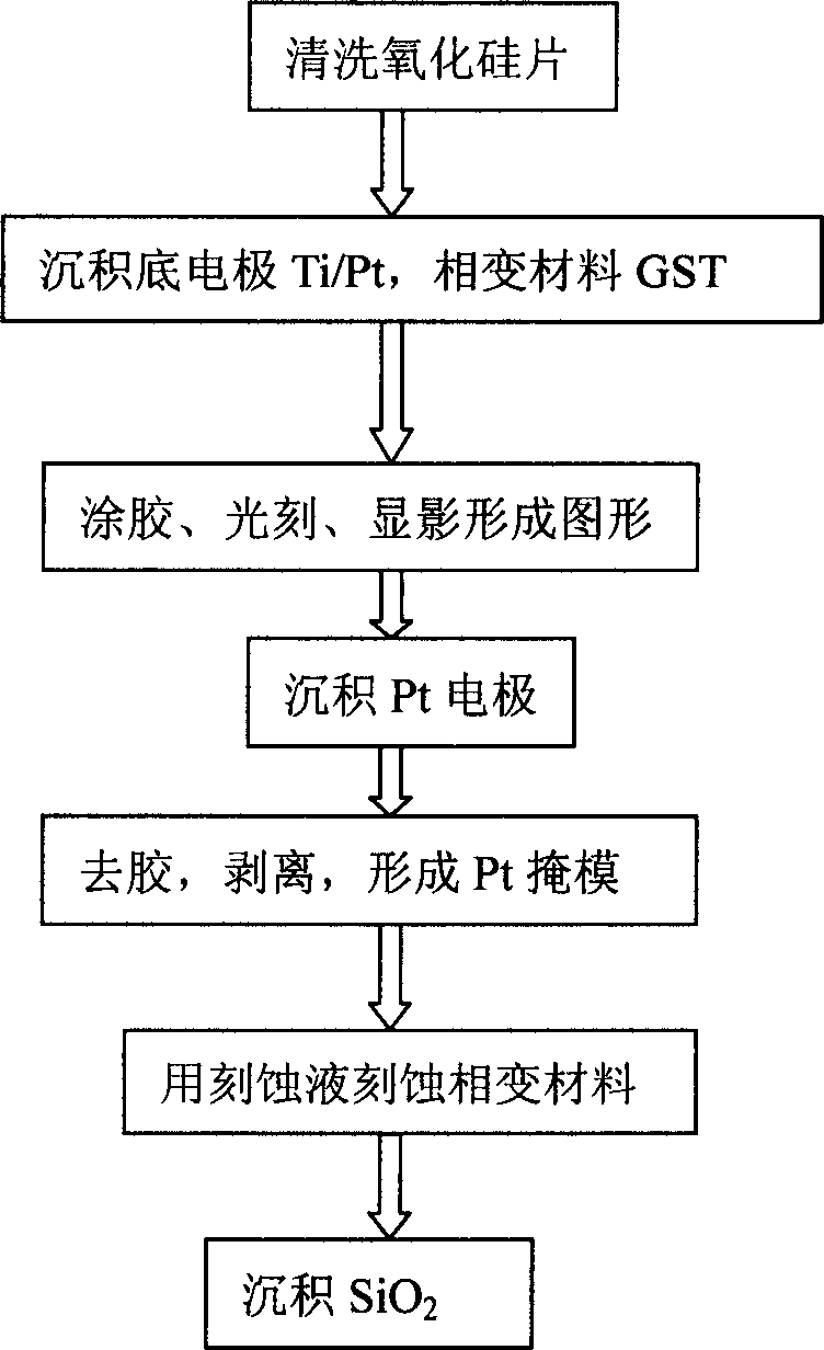
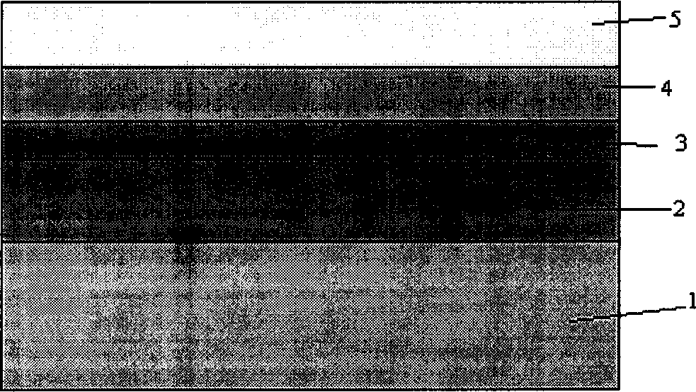
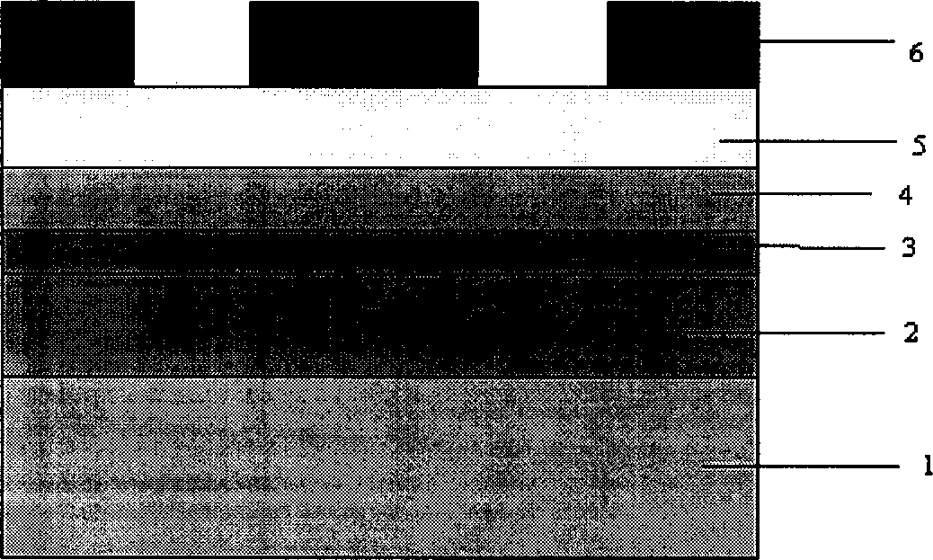
[0033] The silicon oxide wafer is ultrasonically cleaned with acetone, cleaned in the cleaning solution of ammonia water plus hydrogen peroxide, hydrochloric acid plus hydrogen peroxide, respectively, and blown dry with nitrogen after cleaning. Sputter a 30nm metal thin film Ti on a clean silicon oxide wafer with a magnetron sputtering table, then sputter a 100nm metal thin film Pt as the bottom electrode, and finally sputter a 200nm phase change material Ge 2 Sb 2 Te 5 . Coat the sputtered sample with photoresist, place it in a constant temperature box for 35 minutes, then expose it with a photolithography machine for 7 seconds, soak it in chlor...

Embodiment 2

[0038] (1) Configure 50 grams of etchant

[0039] Take 10 grams of tartaric acid, dissolve it in 30 grams of deionized water, add 1 gram of H 2 o 2 , add 1 gram of ethylenediaminetetraacetic acid (EDTA), add 1 gram of fatty alcohol polyoxyethylene ether (JFC), and add deionized water to the rest.

[0040] (2) Prepare etching samples.

[0041] Ultrasonic the silicon oxide sheet with acetone, wash it in ammonia water plus hydrogen peroxide, hydrochloric acid plus hydrogen peroxide cleaning solution, respectively, and dry it with nitrogen after cleaning. Sputter a 50nm metal thin film Ti on a clean silicon oxide wafer with a magnetron sputtering table, then sputter a 100nm metal thin film Pt as the bottom electrode, and finally sputter a 300nm phase change material Ge 2 Sb 2 Te 5 . Coat the sputtered sample with photoresist, place it in a constant temperature box for 30 minutes, then expose it with a photolithography machine for 7 seconds, soak it in chlorobenzene for 5 minut...


PUM


Abstract

Constitution of the etching liquid is as following wtúÑ: 1-30úÑ acid solution, 0.5úÑ-10úÑ oxidant, 0.05úÑ- 10úÑ complexing agent, 0.1-5úÑ surfactant, and other as deionized water. Etching technique includes steps: (1) cleaning out chips of silicon oxide, depositing Ti or TiN, Pt or Au, and film of phase-change material; (2) etching pattern on film of phase-change; (3) depositing Pt or Au; (4) removing unexposed Pt or Au by using debonding technique; (5) etching phase-change material through etching liquid; (6) depositing SiO2 so as to form structure of device. Under condition of controlling etching speed effectively, taking full advantage of positive and lateral etch of etching liquid, the invention prepares Nano structure of phase-change memory through micro processing technique. Advantages are: not polluting device by ion so as to clean device easily, and low cost for treating waste liquor.

Description

technical field [0001] The invention relates to a wet etching agent used in making a phase-change memory and a wet etching process thereof, which belongs to the microelectronic technology in microelectronics. Background technique [0002] Compared with the current dynamic random access memory (DRAM) and flash memory (FLASH), phase-change thin film material random access memory (PRAM) has obvious advantages: it is small in size, low in driving voltage, low in power consumption, fast in read and write speed, and non-volatile . Phase change memory is not only a non-volatile memory, but it is also possible to make multi-level storage, and it is suitable for ultra-low temperature and high temperature environments, and is resistant to radiation and vibration. Therefore, it will not only be widely used in daily portable electronic products, but also in aerospace There are huge potential applications in other fields. In particular, its high speed and non-volatility just make up fo...

Claims


Application Information

Patent Timeline
IPC IPC(8): G03F7/00G03F7/20H01L21/027G11C11/00G11C13/00
Inventor 宋志棠刘奇斌张楷亮封松林陈邦明
Owner SHANGHAI INST OF MICROSYSTEM & INFORMATION TECH CHINESE ACAD OF SCI
Why Eureka
Try Eureka