
Green diode with optical microcavity structure and production thereof

An optical microcavity and diode technology, applied in semiconductor/solid-state device manufacturing, ion implantation plating, coating, etc., can solve the problem of low device brightness, low luminous efficiency and stability, and inevitable redundant holes that do not participate in radiation Composite and other issues

Inactive Publication Date: 2006-08-16
TAIYUAN UNIV OF TECH
View PDF0 Cites 4 Cited by
  • Summary
  • Abstract
  • Description
  • Claims
  • Application Information

AI Technical Summary

Problems solved by technology

[0002] Since the appearance of organic light-emitting diodes in the 1980s, great progress has been made in technology. Due to its advantages of high brightness, high efficiency, low voltage, and DC drive, it has a wide range of applications in the fields of electronics and luminescence. Value, due to its vibrational sidebands and non-uniform broadening effect, the spectral half-width of its organic small molecules and high molecular polymer light-emitting materials is greater than 80nm, so it is used in the preparation of color displays by synthesis of red, green and blue primary colors. Very low, narrow-band emitting rare earth complex luminescent materials, the device has low brightness, low luminous efficiency and stability, and is not as good as devices prepared with broadband emitting materials
[0003] In the existing organic electroluminescent diode devices that emit green light, a single heterostructure is often used, in which the active region is within a narrow range close to the hole transport layer in the electron transport layer. , in the electron transport layer, it is inevitable that there are redundant holes that do not participate in the radiative recombination, and the redundant holes in the electron transport layer are the main internal cause of device aging. The double quantum well structure has obviously improved this, However, the potential barriers and potential wells are cross-stacked, and the luminous brightness and luminous efficiency are not ideal enough to meet the needs of high-grade green diodes for luminous brightness.

Method used


Image

  • Green diode with optical microcavity structure and production thereof
  • Green diode with optical microcavity structure and production thereof
  • Green diode with optical microcavity structure and production thereof

Examples


Embodiment 1

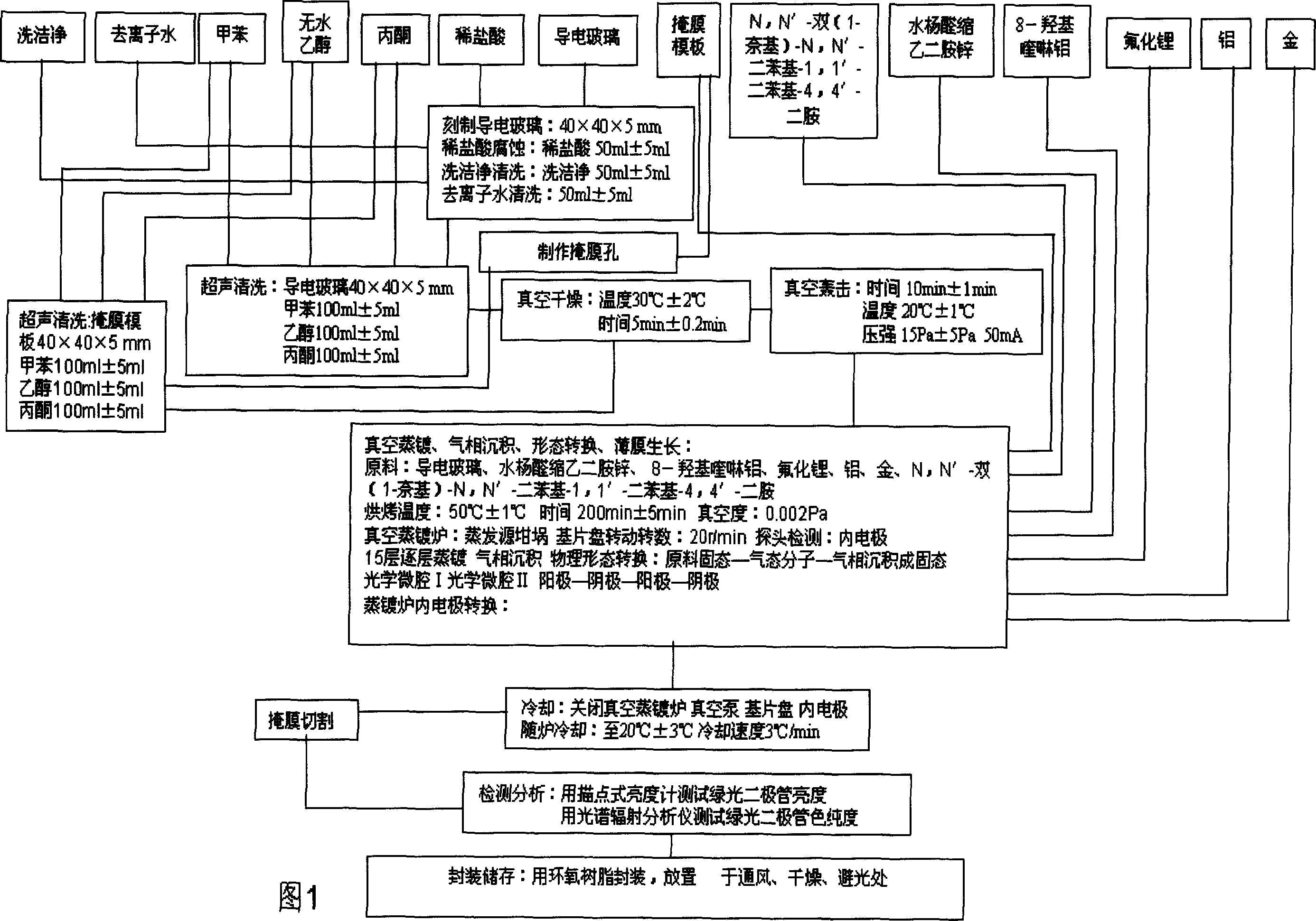
[0131] The vacuum evaporation furnace, console, etching equipment, ultrasonic cleaner, vacuum drying oven, beaker, and container used in the preparation are all in quasi-working condition;

[0132] Selected chemical materials; purity, fineness, precision control, material fineness ≥ 300 mesh, conductive glass square resistance 10Ω / □-60Ω / □, transmittance 80-88%, colorless and transparent, 40×40×5mm , scotch tape 40×2×0.08mm;

[0133] Etching conductive glass: test the conductivity of the front and back sides to determine that the front side is the conductive side;

[0134] Make mask holes: engrave 6 equidistant rectangular through-hole mask holes on the mask template, and the size of the mask holes is 2×2×5mm;

[0135] Etching conductive glass: Paste two transparent tapes symmetrically on the conductive surface, then put in a beaker and add 50ml±5ml of dilute hydrochloric acid, etch for 2min±0.2min, wipe the etched conductive glass with a soft material , peel off the transpar...


PUM

PropertyMeasurementUnit
thicknessaaaaaaaaaa
thicknessaaaaaaaaaa
thicknessaaaaaaaaaa

Abstract

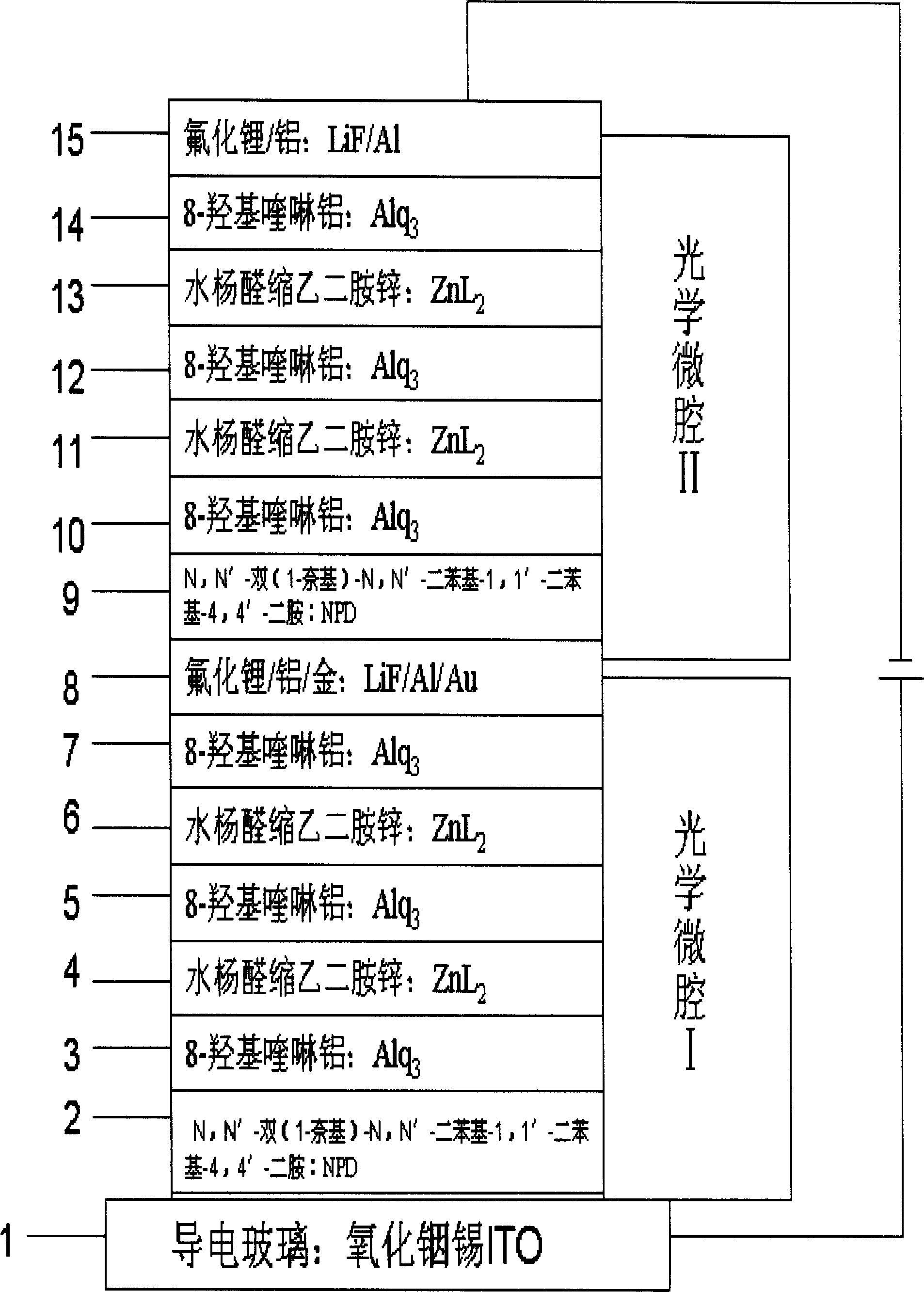
The preparation method takes 8-hydroxyquinoline, N, N'-bis(1-napgthel)-N, N'-diphenyl-1, 1'-dipheny-4, 4'-diamine (NPD), lithium fluoride, aluminum and gold as raw materials, and takes Salicylidenc-Ethylenediamine Zinc as a materials for luminescing green light. The conducting glass tin indium oxide is taken as the substrate of light emitting device. The absolute ethyl alcohol, toluene, acetone, and cleaning agent is taken as detergent. The diluted hydrochloric acid is taken as etching agent. The optical micro-cavity structure of two light-emitting units is adopted, namely 15 layers structure. Through etching conductive glass, cleaning with detergent by ultrasound, drying in vacuum, finely selecting chemical materials, finally the green light emitting diode is acquired. Both thicknesses of potential barrier and potential well in the optical micro-cavity are 3nm+ / -0.5nm. The lithium fluoride / aluminum / gold are used to make intermediate layer with a thickness of 8nm+ / -0.5nm between cathode and anode. The voltages in each layer are evenly and consistent. The green light emitting diode thereof has high luminous efficiency and better green color purity, and the color coordinate is x=0.3246, y=0.5386.

Description

technical field [0001] The invention relates to a green light diode with an optical microcavity structure and a preparation method, and belongs to the technical field of organic metal complex electroluminescent devices and preparation methods. Background technique [0002] Since the appearance of organic light-emitting diodes in the 1980s, great progress has been made in technology. Due to its advantages of high brightness, high efficiency, low voltage, and DC drive, it has a wide range of applications in the fields of electronics and luminescence. Value, due to its vibrational sidebands and non-uniform broadening effect, the spectral half-width of its organic small molecules and high molecular polymer light-emitting materials is greater than 80nm, so it is used in the preparation of color displays by synthesis of red, green and blue primary colors. Very low, narrow-band emitting rare earth complex luminescent materials have low device brightness, low luminous efficiency and...

Claims


Application Information

Patent Timeline
Patent Type & Authority Applications(China)
IPC IPC(8): H01L51/56H01L51/54H01L51/50C23C14/24
Inventor 许并社高志翔郝玉英王华马晨周禾丰刘旭光
Owner TAIYUAN UNIV OF TECH
Learn More