Method for preparing copper conductor for plane display substrate

A flat-panel display, copper wire technology, used in semiconductor/solid-state device manufacturing, semiconductor device, conductive pattern formation, etc., can solve problems such as inability to form metal layers naturally, component operating channel damage, metal wire short-circuits, etc., to avoid short-circuit and Component manipulation channel damage, increased adhesion, low cost effects

Active Publication Date: 2006-08-30
AU OPTRONICS CORP
View PDF1 Cites 7 Cited by
  • Summary
  • Abstract
  • Description
  • Claims
  • Application Information

AI Technical Summary

Problems solved by technology

However, this method cannot naturally form a metal layer with an inclined angle, so it is still necessary to overcome problems such as short circuit of metal wires or damage to device operation channels caused by subsequent etching processes

Method used


Image

  • Method for preparing copper conductor for plane display substrate
  • Method for preparing copper conductor for plane display substrate
  • Method for preparing copper conductor for plane display substrate

Examples


Embodiment 1

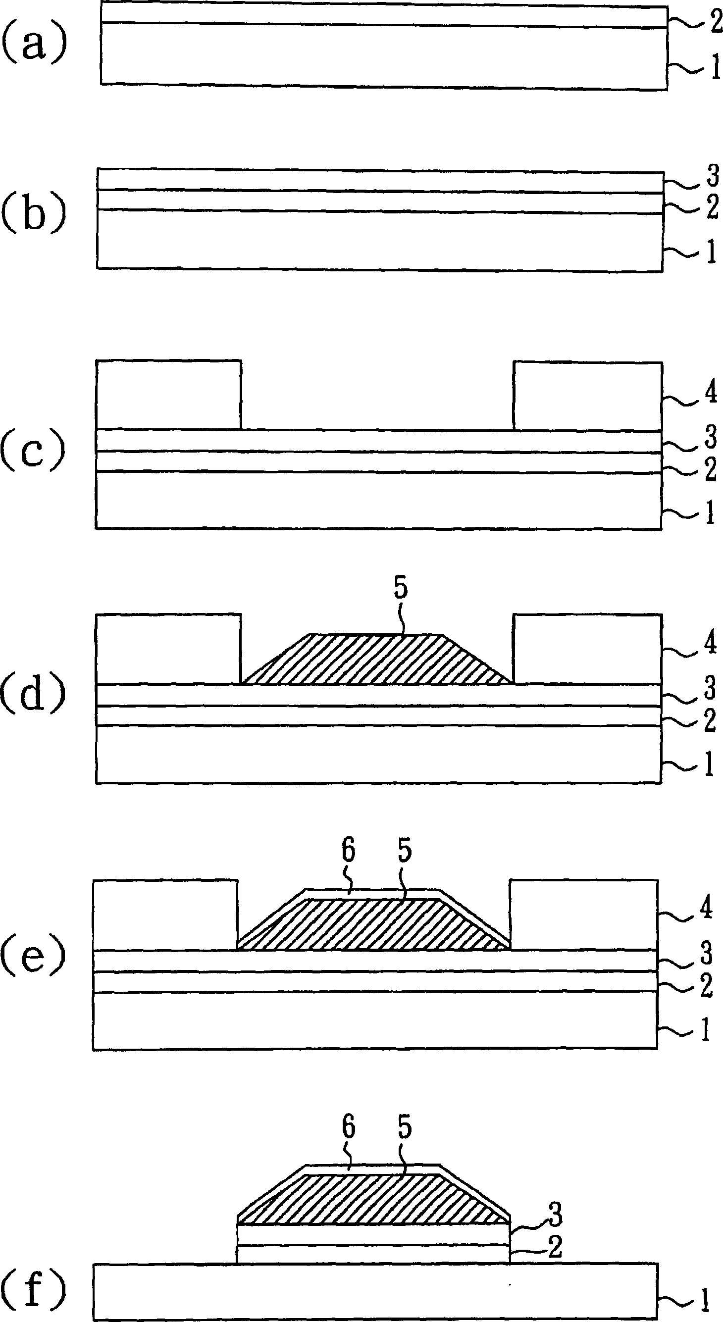
[0035] see figure 2 , figure 2 It is a schematic flow diagram of the copper wire preparation of a preferred embodiment of the present invention. Firstly, an active matrix driven planar display substrate 1 is provided, and a first barrier layer 2 of silicon nitride (TiN) material is deposited on the surface of the substrate 1 by physical vapor deposition, that is, the formation of figure 2 (a) Substrate structure shown. Next, in this embodiment, a physical vapor deposition process is also used to deposit a copper metal seed layer 3 on the surface of the first barrier layer 2 to form a figure 2 (b) Substrate structure shown. Immediately, a positive photoresist layer 4 is deposited on the surface of the copper seed layer 3, and a photomask is used for exposure and development to form a patterned photoresist layer 4, wherein the formed structure is as follows figure 2 (c) shown.

[0036] Depend on figure 2 As shown in (d), the present embodiment obtains the substrate 1...

Embodiment 2

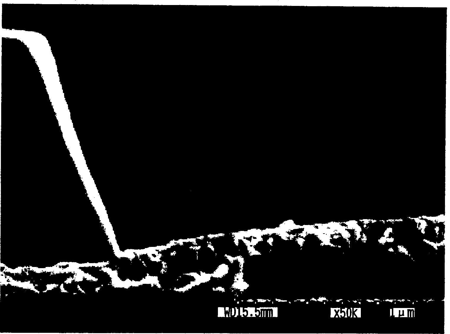
[0040] The preparation method of the copper wire in this embodiment is roughly the same as that shown in Example 1, the only difference being that 90 ppm polydisulfide sodium sulfonate surfactant is added to the electrolyte to form a copper wire layer with an inclination angle 5 , see image 3 The electron micrograph picture shown (the layer on the right side of the figure with an inclination angle of about 25° is the copper wire layer 5 of this embodiment, and the layer on the left side of the figure is the photoresist layer 4 of this embodiment) . In addition, the electroplating condition of the present embodiment is 8ASF (A / ft 2 ), a current density of 100 seconds, and a reaction temperature of 25°C.

Embodiment 3

[0042] The preparation method of the copper wire of this embodiment is roughly the same as that shown in Example 1, the difference is only that 0.75ppm polydisulfide sodium propane sulfonate surfactant and 10ppm polyethylene glycol are added to the electrolyte to form a The copper wire layer 5 with an inclination angle of about 50°. . Therefore, when a little polyethylene glycol and a small amount of sodium polydisulfide dipropane sulfonate are added to the electrolytic solution, the copper wire layer 5 with a complete inclination angle and a flat surface layer can be electroplated and deposited. The electroplating condition of the present embodiment is 10ASF (A / ft 2 ), a current density of 70 seconds, and a reaction temperature of 30°C.


PUM

PropertyMeasurementUnit
Angleaaaaaaaaaa

Abstract

The invention relates to a method for preparing copper leads for a flat display substrate, comprising the steps of: providing a substrate, forming a crystal seed layer on the surface of the substrate, forming a photoresistance layer with pattern on the surface of the crystal seed layer to expose part of the surface of the crystal seed layer and plating a copper lead layer on the partial exposed surface of the crystal seed layer, where the plating electrolyte comprises sulfur-containing compound. In addition, the contact surface between the prepared copper lead layer and the crystal seed layer makes an included angle greater than 0 deg. but less than 90 deg. with the surface of the copper lead layer. Thus, the prepared copper leads can improve the step covering property in the follow-up course and reduce produced holes and form inclined angles without traditional complex etching process.

Description

technical field [0001] The invention relates to a method for preparing a copper wire for a plane display substrate, in particular to a method for preparing a copper wire suitable for an electrode or a metal wire for a thin film transistor of a plane display substrate. Background technique [0002] In order to increase the transmission speed of the driving signal of the thin film transistor, in order to meet the needs of the current color flat-panel display with increasing size and high image quality, copper metal with low resistivity can be used as the metal wire or gate electrode of the flat-panel display substrate to Solve the problem of driving signal delay. [0003] However, there are still problems to be overcome in the application of copper materials, such as: easy oxidation and moisture corrosion, poor adhesion, interlayer diffusion, etc., so multi-layer structures are often used to solve the above shortcomings, but the copper wires of this multi...

Claims


Application Information

Patent Timeline
IPC IPC(8): H01L21/768H01L21/28H05K3/10
Inventor 郑湘宁李泓伟朱闵圣万其超王咏云刘柏村
Owner AU OPTRONICS CORP
Why Eureka
Try Eureka