Method for improving solar energy conversion efficiency using metal oxide photocatalysts having energy band of core-shell for ultraviolet ray and visible light absorption and photocatalysts thereof
a technology photocatalysts, which is applied in the direction of catalyst activation/preparation, metal/metal-oxide/metal-hydroxide catalysts, etc., can solve the problems of low electron-hole formation efficiency, low numerical value of solar energy conversion efficiency, and large number of electron-holes participating in the final redox reaction. achieve the effect of maximizing the catalyst characteristics of metal oxide, increasing the electron carrier density, and extending the wavelength wavelength wavelength
- Summary
- Abstract
- Description
- Claims
- Application Information
AI Technical Summary
Benefits of technology
Problems solved by technology
Method used
Image
Examples
example 1
[0048]A method of fabricating a photoelectrochemical electrode is as follows. 100 mg of anatase TiO2 nanoparticles having a particle diameter of about 25 nm was sufficiently dispersed in 50 ml of acetone solution containing 20 mg of iodine dissolved therein. Two nickel foils were immersed in the prepared solution so as to face each other, and then, 100V DC was applied to the same for 1 minute, to form a TiO2 nanoparticle thin film layer having a thickness of about 250 nm on the nickel foil side of a cathode. The TiO2 thin film sample was subjected to heat treatment at 500° C. in an air atmosphere for 40 minutes to improve adhesion between the thin film layer and the nickel foil substrate and, at the same time, to remove organic impurities formed in the thin film fabrication process. A variety of metal oxides such as V, Fe, Cu, Zn, Ta, W or Bi, etc. metal oxide nanoparticles (<50 nm) may also be fabricated into a photoelectrochemical electrode by the same process as described above.
[...
experimental example
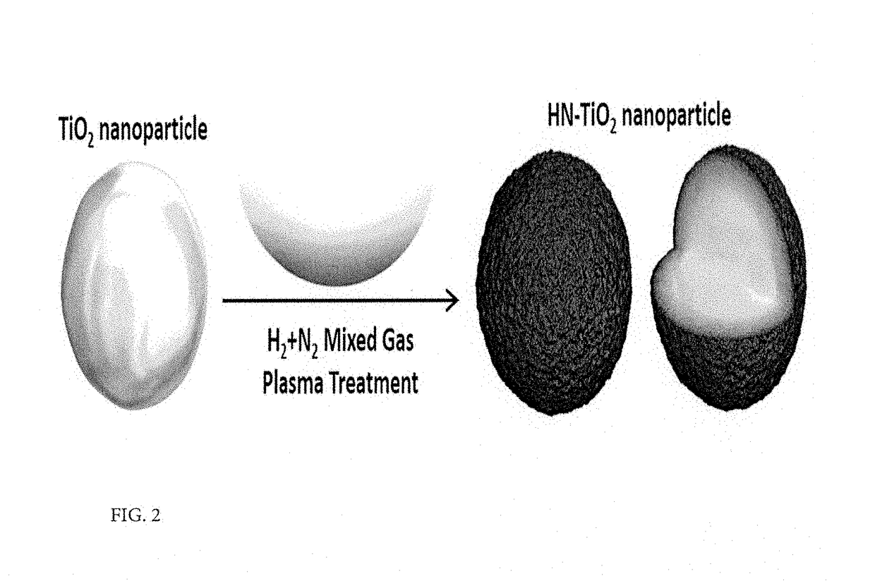
[0052]FIG. 4 illustrates changes in light absorbance and crystallinity between a TiO2 nanoparticle (HN—TiO2) on which mixed gas plasma treatment was executed according to the above-described method and a TiO2 nanoparticle (bare TiO2) without any treatment. As shown in the inset of FIG. 4a, a conventional white TiO2 thin film changed into a dark yellow color by the plasma treatment and showed a great increase in light absorbance characteristics in a visible light region after plasma treatment, as observed in the light absorbance curve of each sample in FIG. 4a, which was prepared using the Tauc relationship. As a result of calculating a size of the band-gap for each sample using x intercepts of the graph shown in FIG. 4a, it was observed that the bare TiO2 had 3.27 eV while HN—TiO2 showed a decrease to 2.71 eV. Further, existence of an additional band-gap with a size of 1.92 eV was observed.
[0053]FIGS. 4c and 4d illustrate transmission electron microscopy (TEM) photographs of a singl...
PUM
| Property | Measurement | Unit |
|---|---|---|
| temperature | aaaaa | aaaaa |
| temperature | aaaaa | aaaaa |
| temperature | aaaaa | aaaaa |
Abstract
Description
Claims
Application Information


