Flip chip assembly structure for semiconductor device and method of assembling therefor

Inactive Publication Date: 2002-05-16
HITACHI LTD
View PDF0 Cites 128 Cited by
  • Summary
  • Abstract
  • Description
  • Claims
  • Application Information

AI Technical Summary

Problems solved by technology

In the assembly structure by the conventional assembly method 1), it is difficult due to the problem such as the heat resistance or the like of the under fill resin to increase the heating temperature so that the metallic joining between the bumps and the pads (in the present specification, the joining at the atom level is referred to as the metal joining) is not achieved.
In such a case, if the connection resistance is large, then it becomes difficult to operate normally the circuits on the chop.
In addition, the loss due to the resistances in the connection parts is large, and hence it becomes a problem in terms of the power consumption.
Also, if resin draws the moisture to expand under the environment of the high temperature and the high humidity, then the resistance is increased, and in the extreme case, the malconduction is caused.
This becomes a problem in terms of the reliability as well.
In the assembly structure by the conventional assembly method 2), since the electrical conduction is ensured on the basis of the contact between the electrically conductive particles, there arises a problem that it is difficult to achieve the metal joining and hence the electrical resistance in each of the connection parts is large.
In addition, when each of the bumps becomes minute, the number of electrically cond

Method used


Image

  • Flip chip assembly structure for semiconductor device and method of assembling therefor
  • Flip chip assembly structure for semiconductor device and method of assembling therefor
  • Flip chip assembly structure for semiconductor device and method of assembling therefor

Examples


first embodiment

[0054] (First Embodiment)

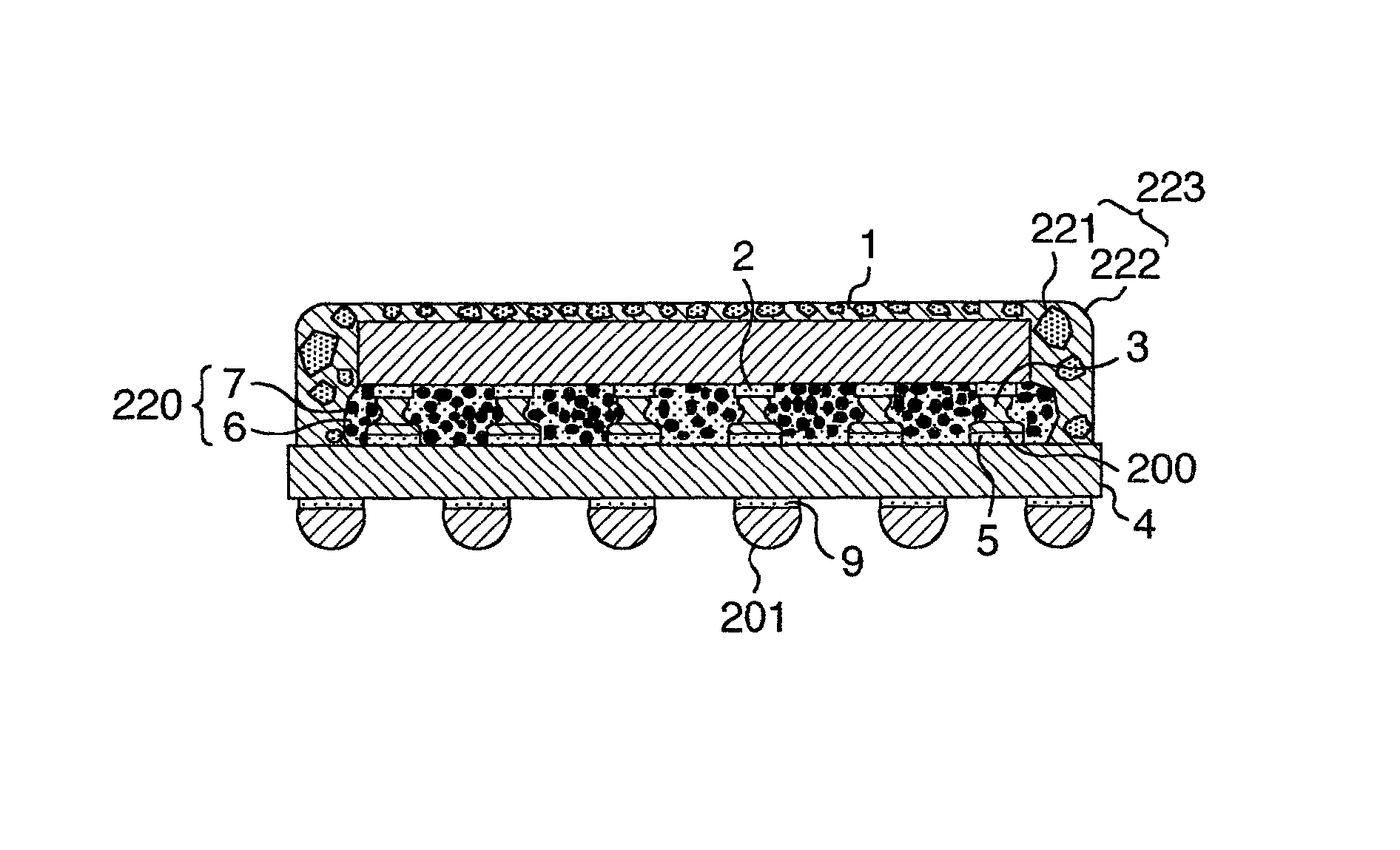
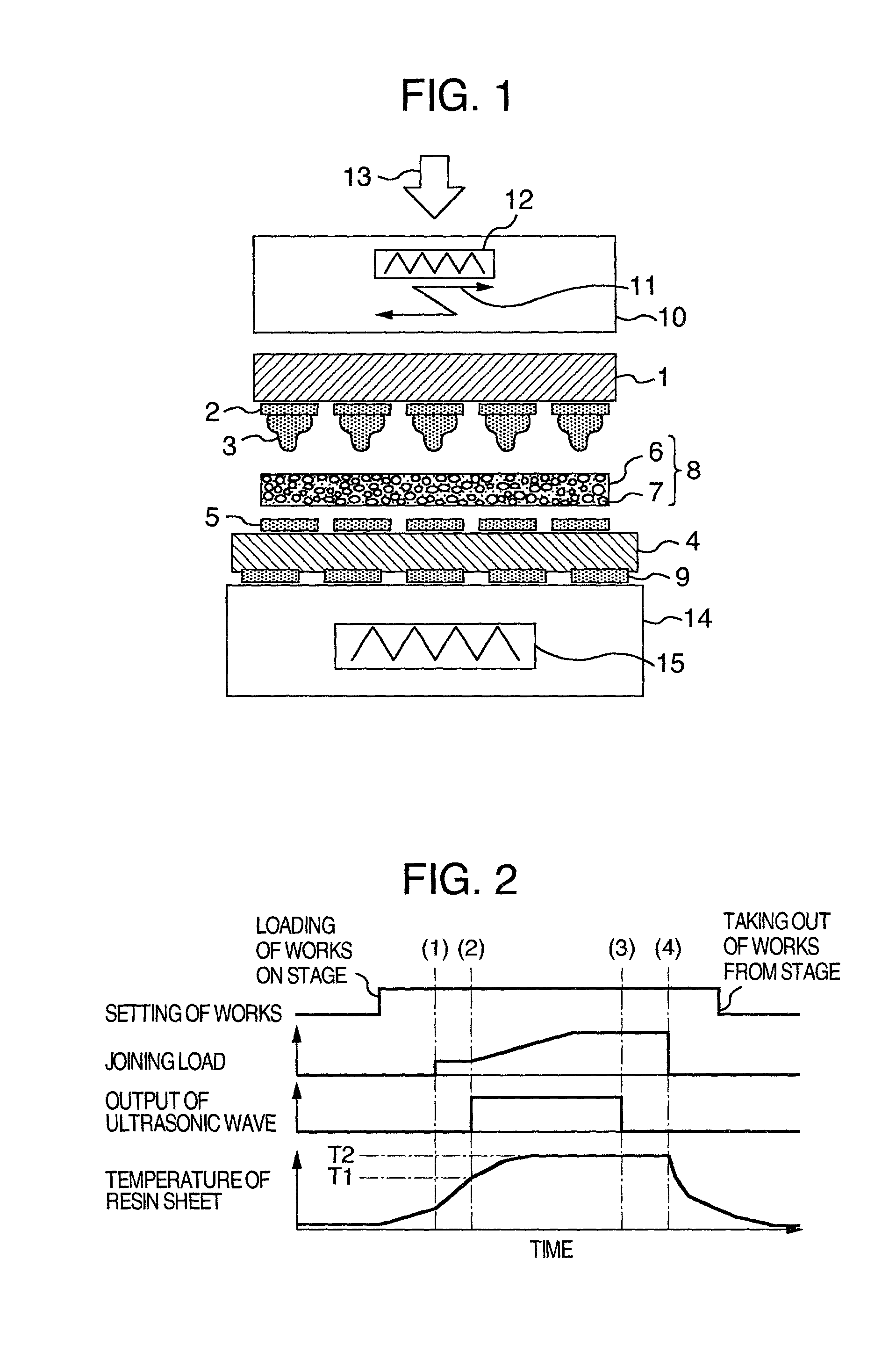
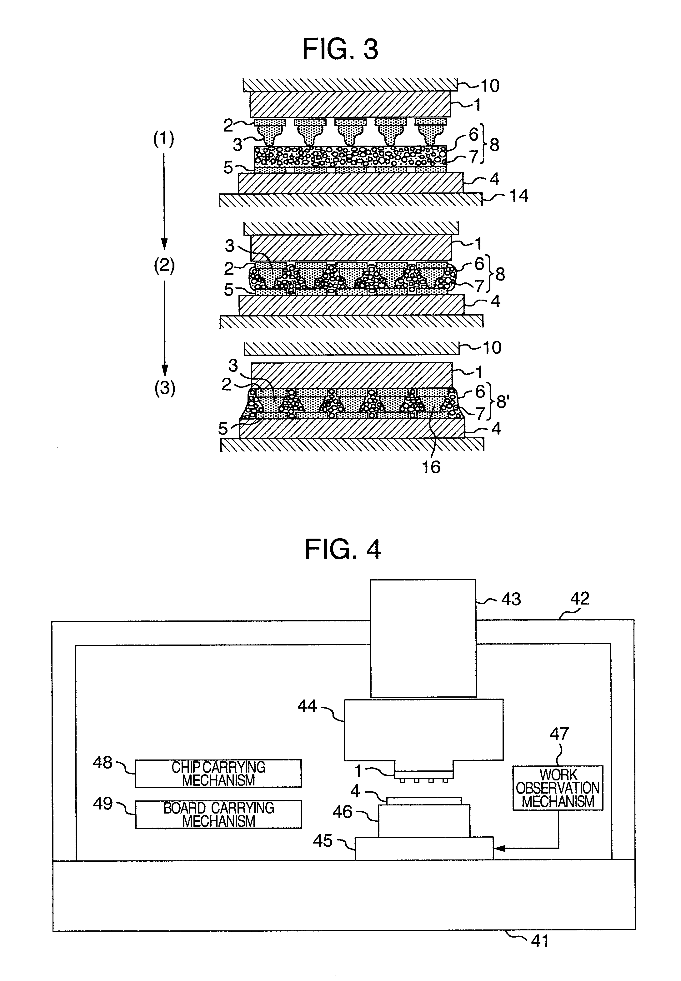
[0055] FIG. 1 shows the construction of joining members and the periphery of the joining members in assembling a flip chip using the ultrasonic wave according to the present invention. In the figure, Au bumps 3 are respectively formed on electrodes 2 of a semiconductor chip 1. The Au bumps are formed by utilizing the ball bonding method. Each of them has two-steps projection type shape in which the height there of is increased as the position thereon is nearer the center of the bump and is formed in such a way that the diameter is 100 .mu.m, the head height is 100 .mu.m, the shoulder height of the first step (on the side of the semiconductor chip 1) is 30 .mu.m and the diameter of the second step (on the side of an organic printed circuit board 4) is 40 .mu.m. On the other hand, after the surfaces of internal connection terminals 5 containing Cu as the basic constituent have been plated with Ni, an Au plated film with 0.7 .mu.m thickness is formed thereon. E...

second embodiment

[0083] (Second Embodiment)

[0084] As another embodiment, instead of sandwiching the resin sheet in the semi-cured state in the first embodiment between the chip and the board, the liquid epoxy resin with about 50 .mu.m thickness containing the insulating inorganic fillers (SiO.sub.2: the mean particle size is 1 .mu.m, and the maximum value is 7 .mu.m) is applied to the chip mounting area of the board, and thereafter immediately, the chip with the Au bumps is mounted on the liquid resin to carry out the ultrasonic wave joining, and subsequently, the curing processing at 150 degrees for 30 minutes is carried out. In the case of the liquid resin, while the pad surfaces of the board are contaminated with the resin, the joining condition is made the condition of the heavy load or the high ultrasonic wave power, whereby it is confirmed that the partial metallic joining can be achieved. In this connection, as for the liquid resin, in addition to the epoxy resin, other thermosetting resin su...

third embodiment

[0088] (Third Embodiment)

[0089] FIG. 9 shows an embodiment of the flip chip assembly method according to the present invention. In the figure, the Au bumps 3 are respectively formed on the electrodes (the Al electrodes) 2 of the chip 1 by utilizing the ball bonding method. At this time, the initial bump diameter is 60 .mu.m, the diameter in the second step is 35 .mu.m, the bump height is 80 .mu.m, and the shoulder height in the first step is 10 .mu.m. Two sheets of resin sheets are employed. Then, a high filler containing epoxy resin sheet (a low thermal expansion resin sheet) 90 in which the containing rate of the fillers 7 made of spheroidal SiO.sub.2 particles is 65% is arranged on the chip side, while a low filler containing epoxy resin sheet (an intermediate thermal expansion resin sheet) 91 in which the containing rate of the same fillers as those of the former is 35% is arranged on the board side in order to carry out the lamination. An Au film with 0.5 .mu.m thickness is for...


PUM


Abstract

A semiconductor device includes a semiconductor chip and a printed circuit board. Metal electrodes of the semiconductor chip and the internal connection terminals of the printed circuit board are electrically connected through the metallic joining via precious metal bumps. A melting point of a metal material constituting each of the metallic joining parts is equal to or higher than 275 degrees, and a space defined between the chip and the board is filled with resin (under fill) containing 50 vol % or more inorganic fillers.

Description

[0001] 1. Field of the Invention[0002] The present invention relates to flip chip assembly structure for a semiconductor chip in which each of precious metal bumps is employed as a material for electrical connection.[0003] 2. Description of the Related Art[0004] As for the conventional flip chip assembly method employing Au bumps, 1) the assembly method wherein insulating resin is applied to an insulating board, the position of the insulating board is made align with the position of a semiconductor element, the load is applied to make the projection electrodes of the semiconductor element contact the conductor wiring of the insulating board and also then the insulating resin is cured to carry out the connection is described in JP-A-2-28946, and 2) the assembly method wherein the heating is carried out through an anisotropic conductive adhesive and also both of the pressure and the ultrasonic wave are applied to connect bumps which are formed on a chip and electrodes of a board to ea...

Claims


Application Information

Patent Timeline
IPC IPC(8): H01L21/52H01L21/56H01L21/60H01L21/607H01L23/29H01L23/31H01L23/485
CPCH01L21/563H01L23/295H01L24/31H01L24/75H01L24/81H01L2224/1134H01L2224/13099H01L2224/13144H01L2224/16145H01L2224/16225H01L2224/48227H01L2224/48471H01L2224/48479H01L2224/73203H01L2224/73204H01L2224/75H01L2224/75314H01L2224/75745H01L2224/75753H01L2224/81205H01L2224/81409H01L2224/81801H01L2224/83101H01L2224/85051H01L2224/85444H01L2924/01004H01L2924/01005H01L2924/01013H01L2924/01022H01L2924/01025H01L2924/01029H01L2924/01033H01L2924/01046H01L2924/01047H01L2924/01049H01L2924/0105H01L2924/01078H01L2924/01079H01L2924/01082H01L2924/01322H01L2924/15153H01L2924/15165H01L2924/15311H01L2924/19105H01L2924/30107H01L2924/0132H01L24/29H01L2224/32225H01L24/48H01L2924/01006H01L2924/01075H01L2924/014H01L2224/29386H01L2224/32145H01L2224/45144H01L2924/1579H01L2224/29111H01L2224/2929H01L2224/81191H01L2924/10253H01L2224/293H01L2224/83851H01L2924/12041H01L2924/07811H01L2224/16227H01L24/45H01L24/11H01L24/13H01L2224/29082H01L2224/83192H01L2224/83193H01L2224/29499H01L2224/325H01L2924/00H01L2924/3512H01L2924/00014H01L2924/05442H01L2924/0665H01L2224/73265H01L2924/351H01L2924/15787H01L2924/181H01L2224/48644H01L24/73H01L2924/15151H01L2924/18161H01L2224/11H01L2224/13H01L2224/05573H01L2224/05568H01L2224/75317H01L2924/00012H01L2224/05624H01L2224/4554H01L21/52
Inventor KAJIWARA, RYOICHIKOIZUMI, MASAHIROMORITA, TOSHIAKITAKAHASHI, KAZUYANISHIMURA, ASAOSHINODA, MASAYOSHI
Owner HITACHI LTD
Why Eureka
Try Eureka