Electron-emitting device, cold cathode field emission device and method for production thereof, And cold cathode field emission display and method for production thereof

Inactive Publication Date: 2002-06-27
SONY CORP
View PDF5 Cites 55 Cited by
  • Summary
  • Abstract
  • Description
  • Claims
  • Application Information

AI Technical Summary

Benefits of technology

0028] It is therefore an object of the present invention to provide an electron-emitting device and a cold cathode field emission device that permit electron emission in a far lower electric field, make it possible to decrease the temperature to be employed for forming an electron emitting portion and have the el

Problems solved by technology

For applying the liquid crystal display to a floor-type television receiver, however, it still has problems to be solved concerning a higher brightness and an increase in size.
That is, it is very difficult to form the electrically conductive material layer 218 having a uniform quality and a uniform thickness on the entire support member having a large area by a vertical deposition method or to form the peel-off layer 217 having uniform dimensions and having the form of eaves by an oblique deposition method, and some in-plane fluctuation or some fluctuation among lots is inevitable.
Further, when the peel-off layer 217 formed on a large area is removed, its residue causes the cathode panel CP to be contaminated, and there is caused a problem that the manufacturing yield of displays is decrease

Method used


Image

  • Electron-emitting device, cold cathode field emission device and method for production thereof, And cold cathode field emission display and method for production thereof
  • Electron-emitting device, cold cathode field emission device and method for production thereof, And cold cathode field emission display and method for production thereof
  • Electron-emitting device, cold cathode field emission device and method for production thereof, And cold cathode field emission display and method for production thereof

Examples


example 2

[0170] Example 2 is concerned with the field emission device according to the first constitution and the display according to the first constitution, and it is also concerned with the production method according to the first constitution A.

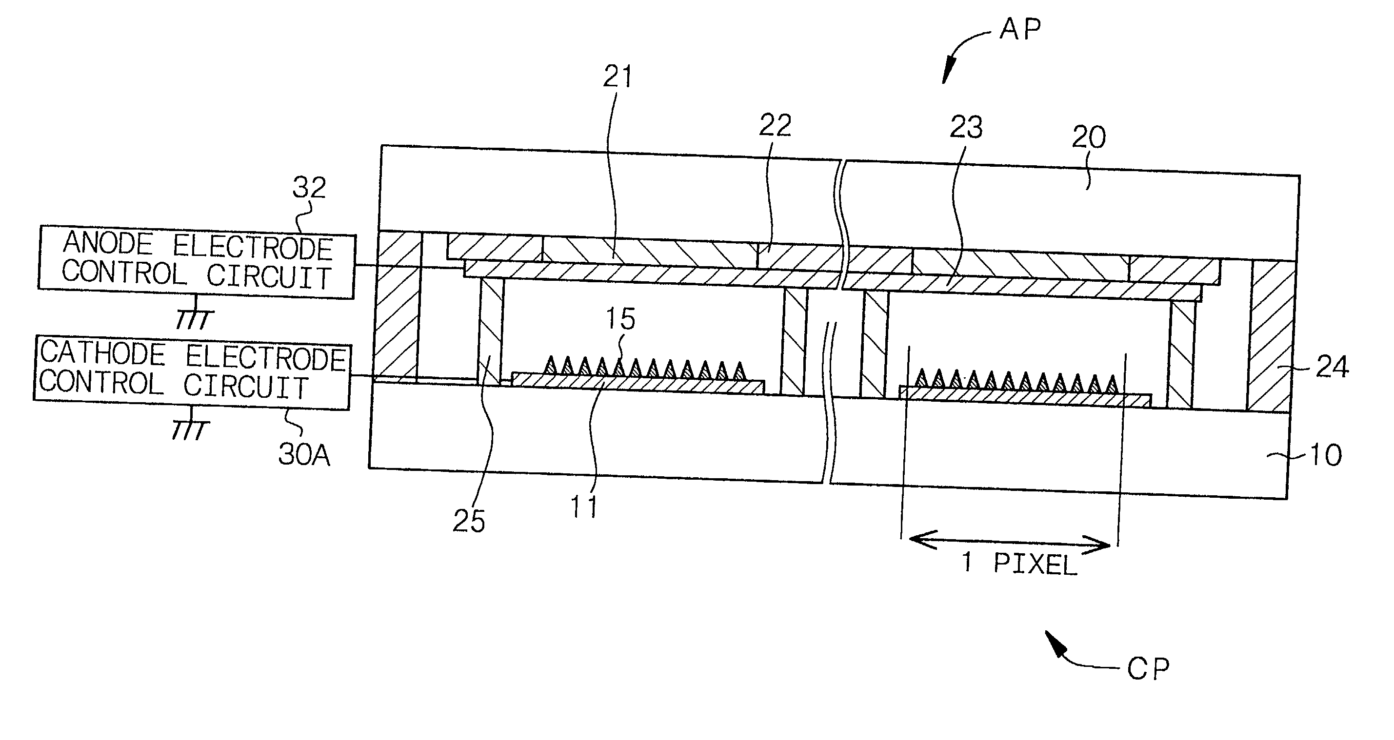
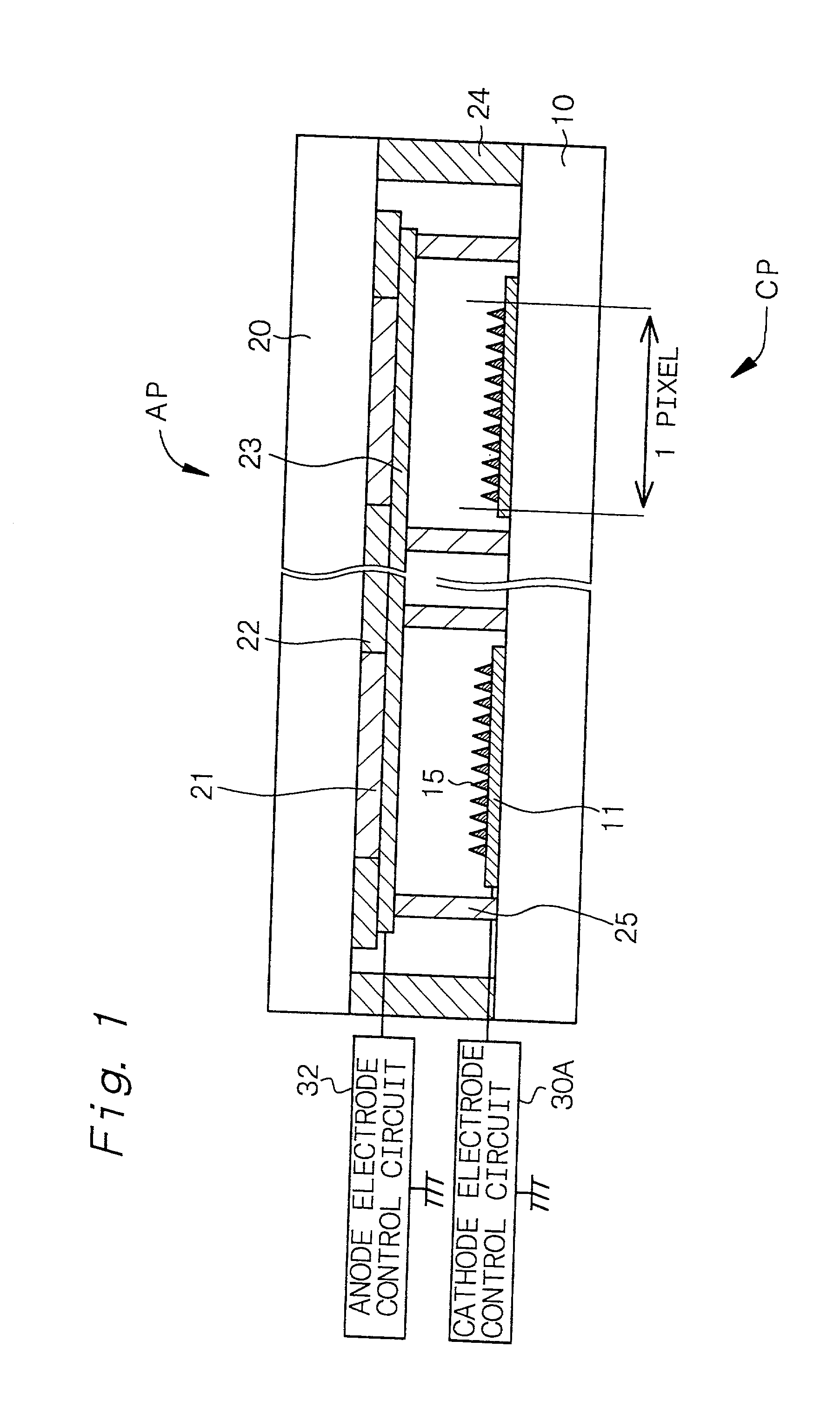
[0171] FIG. 9 shows a schematic partial end view of the display in Example 2, FIG. 6C and FIG. 8 show schematic partial cross-sectional views of the field emission device, and FIG. 7 shows a layout of the separation walls, the cathode electrodes and the gate electrodes in the field emission devices. While FIG. 9 shows one electron emitting portion 15 exposed in the bottom of an opening portion 114A, many electron emitting portions 15 are exposed in an actual embodiment.

[0172] In Example 2, as is shown in the schematic partial cross-sectional view of FIG. 6C, the field emission device further has a gate electrode 113 having an opening portion 114A, and the electron emitting portions 15 are selectively formed on that portion of the cathode electrode...

example 3

[0191] Example 3 is concerned with the field emission device according to the second constitution and the display according to the second constitution, and it is also concerned with the production method according to the first constitution B of the present invention.

[0192] In Example 3, as is shown in the schematic partial end view of FIG. 12, an insulating layer 12 is formed on the support member 10 and the cathode electrode 11, a gate electrode 13 is formed on the insulating layer 12, a second opening portion 14B communicating with a first opening portion 14A formed in the gate electrode 13 is formed in the insulating layer 12, and electron emitting portions 15 are exposed in the bottom of the second opening portion 14B. The electron-emitting device, the field emission device and the display in Example 3 can be constitutionally the same as those in Example 1 except for the above points, so that detailed explanations thereof are omitted. FIG. 13 shows a schematic partial end view o...

example 4

[0215] Example 4 is concerned with the field emission device according to the second constitution and the display according to the second constitution, and it is also concerned with the production method according to the first constitution C of the present invention. The field emission device in Example 4 is structurally the same as that explained in Example 3, so that detailed explanations thereof are omitted.

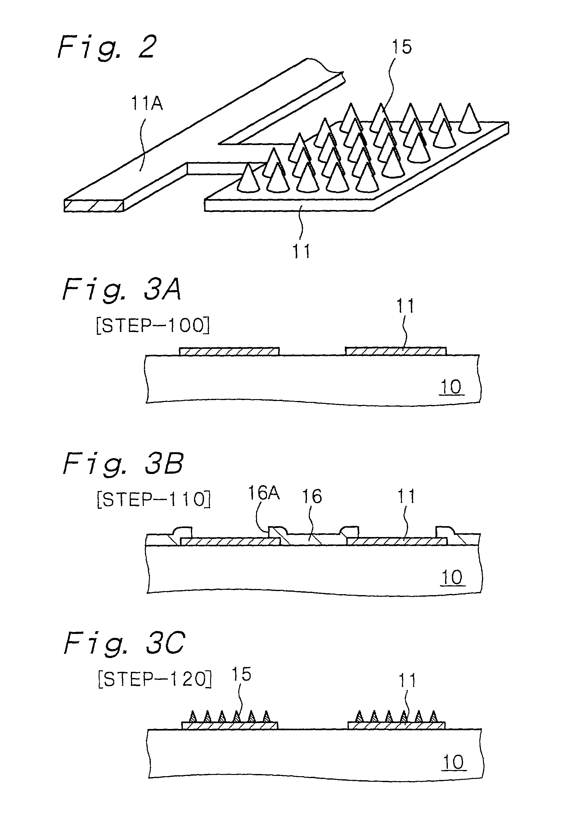
[0216] The method of producing the field emission device and the method of producing the display in Example 4, which are production methods according to the first constitution C of the present invention, will be explained with reference to FIGS. 15A to 15C hereinafter. In Example 4, the field emission device is formed by the steps of;

[0217] forming the cathode electrode 11 on the support member 10,

[0218] selectively forming the conical electron emitting portion 15 made of carbon on the surface of the cathode electrode 11,

[0219] forming an insulating layer 12 on the support mem...


PUM


Abstract

A cold cathode field emission device comprising a cathode electrode formed on a support member, and a conical electron emitting portion made of carbon and formed on the cathode electrode.

Description

BACKGROUND OF THE INVENTION AND RELATED ART STATEMENT[0001] The present invention relates to an electron-emitting device, a cold cathode field emission device and a method for the production thereof, and it also relates to a cold cathode field emission display and a method for the production thereof.[0002] In the fields of displays for use in television receivers and information terminals, studies have been made for replacing conventionally mainstream cathode ray tubes (CRT) with flat-panel displays which are to comply with demands for a decrease in thickness, a decrease in weight, a larger screen and a high fineness. Such flat panel displays include a liquid crystal display (LCD), an electroluminescence display (ELD), a plasma display panel (PDP) and a cold cathode field emission display (FED). Of these, a liquid crystal display is widely used as a display for an information terminal. For applying the liquid crystal display to a floor-type television receiver, however, it still has...

Claims


Application Information

Patent Timeline
IPC IPC(8): H01J1/304H01J3/02H01J1/30H01J9/02H01J29/04H01J31/12
CPCH01J9/025H01J3/022H01J1/30
Inventor INOUE, KOUJIMUROYAMA, MASAKAZUYAGI, TAKAO
Owner SONY CORP
Why Eureka
Try Eureka