Semiconductor device and method of manufacturing the semiconductor device

a semiconductor and semiconductor technology, applied in the direction of semiconductor devices, electrical devices, transistors, etc., can solve the problems of increasing parasitic capacitance, poor heat resistance of materials, and etching of gate wiring lines under alumina films

Inactive Publication Date: 2002-07-25
SEMICON ENERGY LAB CO LTD
View PDF0 Cites 220 Cited by
  • Summary
  • Abstract
  • Description
  • Claims
  • Application Information

AI Technical Summary

Problems solved by technology

Moreover, with respect to the source wiring line and gate wiring line, since a TFT is connected to each of pixels and the number of pixels is increased, increase of parasitic capacitance also becomes a problem.
While the aluminum material has the merit of low resistance, the material has the demerit of poor heat resistance.
However, buffered hydrofluoric acid has a small selection ratio of alumina (typically Al.sub.2O.sub.3) to aluminum, so that there is a problem that not only the alumina film but also the gate wiring line under the alumina film is etched.
That is, if the state as shown in FIG. 30 occurs, the contact area between wiring lines is extremely reduced, so that electrical connection becomes almost impossible.
Thus, it becomes impossible to operate the TFT and causes an erroneous operation of a circuit itself.
However, in view of the fact that a large amount of heavy metal chromium, which has a possibility to damage a human body, is required to be used, the process of using chromium mixed acid is not desirable in industry.
However, this technique has a problem that a material used for crystallization remains in the crystalline silicon film, and the material has a bad influence on the component characteristics (especially, reliability, uniformity, and the like) of a TFT.
However, in the above gettering technique, since the aluminum material having low heat resistance is used for the wiring line, a heat treatment is restricted within a temperature range (about 300 to 450.degree. C.).
Since the above temperature range is low as a temperature at which the material in the crystalline silicon film is sufficiently guttered, a long treatment time is required.
), aluminum atoms diffuse into a gate insulating film and reach a channel formation region, so that the atoms have caused a bad operation of a TFT or lowering of TFT characteristics.
Similarly, even in the heating treatment within the above temperature range, protrusions, such as hillocks or whiskers, produced from the aluminum m...

Method used


Image

  • Semiconductor device and method of manufacturing the semiconductor device
  • Semiconductor device and method of manufacturing the semiconductor device
  • Semiconductor device and method of manufacturing the semiconductor device

Examples


embodiment 2

[0215] Embodiment 1, although the explanation has been given to the case, where the NTFT is manufactured, as an example, it is needless to say that the present invention can be applied to a PTFT. If a well-known CMOS technique is used, it is also easy to constitute a CMOS circuit in which an NTFT and a PTFT are complementarily combined.

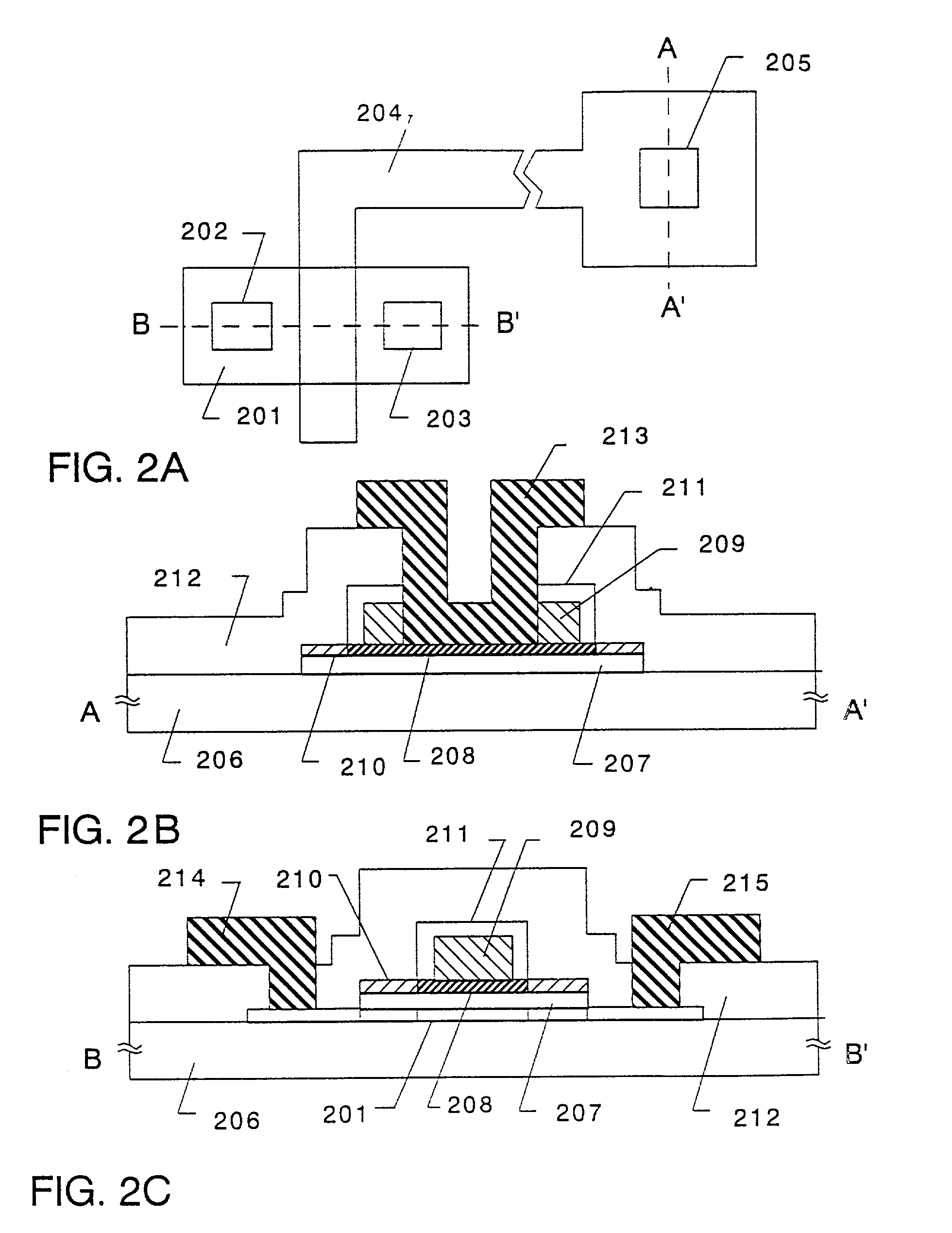
[0216] In this embodiment, an example in which an active matrix substrate comprising a driving circuit constituted by CMOS circuits and a pixel matrix circuit constituted by NTFTs formed on the same substrate is manufactured, will be described with reference to FIG. 7.

[0217] In FIG. 7, an NTFT 501 and a PTFT 502 constitute a CMOS circuit 503. As described before, if a well-known CMOS technique is used, this embodiment can be easily realized by almost the same steps as the embodiment 1.

[0218] A pixel TFT (in this embodiment, NTFT) 504 constituting the pixel matrix circuit can be realized by adding some steps to the manufacturing steps explained in the ...

embodiment 3

[0228] Manufacturing steps of a TFT using the present invention will be described with reference to FIGS. 4A-4E, 5A-5C, 6A, and 6B. In this embodiment, an example in which an N-channel TFT (NTFT) is manufactured, is shown. The present invention has a feature in steps from formation of a gate electrode to formation of source / drain regions, and other portions can be formed by a well-known technique. Thus, the present invention is not limited to the manufacturing steps of this embodiment.

[0229] First, a glass substrate (Corning 1737; distortion point=667.degree. C.) was prepared as a substrate 401, and a silicon oxide film with a thickness of 200 nm was formed as an under film 402 on the substrate. An active layer 403 with a thickness of 45 nm was formed on the under film by a well-known means. The thickness of the active layer 403 is made 10 to 100 nm (preferably 15 to 75 nm, more preferably 20 to 45 nm) (FIG. 4A).

[0230] The active layer 403 was formed of a polycrystalline silicon fil...

embodiment 4

[0275] In the embodiment 3, although the explanation has been given to the case, where the NTFT is manufactured, as an example, it is needless to say that the present invention can be applied to a PTFT. An example of manufacturing steps of the P-channel type TFT (PTFT) and manufacturing conditions will be described in brief below.

[0276] First, an impurity ion (boron) to impart P-type conductivity is implanted into source and drain regions where phosphorus ions were implanted. As a doping gas, diborane diluted to 5% with hydrogen is used. The acceleration voltage is made 60 to 90 keV, and the dosage is made 1.times.10.sup.13 to 8.times.10.sup.15 atoms / cm.sup.2. It is important to adjust the dosage such that the concentration obtained by subtracting the maximum value of the concentration of phosphorus from the maximum value of the concentration of boron implanted in the source and drain regions becomes 3.times.10.sup.19 to 3.times.10.sup.21 atoms / cm.sup.3. As a result, the conductivit...


PUM


Abstract

A TFT using an aluminum material for a gate electrode is manufactured at a high yield factor. The gate electrode provided over an active layer and a gate insulating film is constituted by a lamination film of a tantalum layer and an aluminum layer. In this structure, the tantalum layer functions as a stopper, so that it is possible to prevent a constituent material of the aluminum layer from intruding into the gate insulating film. An end portion of the tantalum layer is transformed into tantalum oxide, which has an effect to lower damage at ion implantation to the gate insulating film in the formation of an LDD region.

Description

[0001] 1. Field of the Invention[0002] The present invention relates to the structure of a semiconductor device including a semiconductor circuit constituted by a plurality of insulated gate type transistors, such as thin film transistors using semiconductor thin films, and to a method of manufacturing the same. The semiconductor device of the present invention includes also an electronic equipment having a semiconductor circuit constituted by insulated gate type transistors, such as an active matrix type liquid crystal display device and an image sensor.[0003] 2. Description of the Related Art[0004] In recent years, attention has been paid to an active matrix type liquid crystal display device (hereinafter abbreviated to AMLCD) in which a pixel matrix circuit and a driving circuit are constituted by TFTs formed on an insulating substrate.[0005] As an insulating substrate, it is desired to use an inexpensive glass substrate rather than using an expensive substrate, such as a quartz ...

Claims


Application Information

Patent Timeline
IPC IPC(8): H01L21/336H01L29/45H01L29/49H01L29/786
CPCH01L29/458H01L29/4908H01L29/66757H01L29/78621
Inventor YAMAZAKI, SHUNPEIOHTANI, HISASHIFUJIMOTO, ETSUKOFUKUNAGA, TAKESHIADACHI, HIROKIOHNUMA, HIDETO
Owner SEMICON ENERGY LAB CO LTD
Why Eureka
Try Eureka