

Polishing pad, method of manufacturing the polishing pad, and cushion layer for polishing pad
a cushion layer and polishing pad technology, applied in the field of polishing pads, can solve the problems of poor cushioning characteristics, difficult to give uniform pressure onto the whole surface of the wafer, and high polishing ra
- Summary
- Abstract
- Description
- Claims
- Application Information
AI Technical Summary
Benefits of technology
Problems solved by technology
Method used
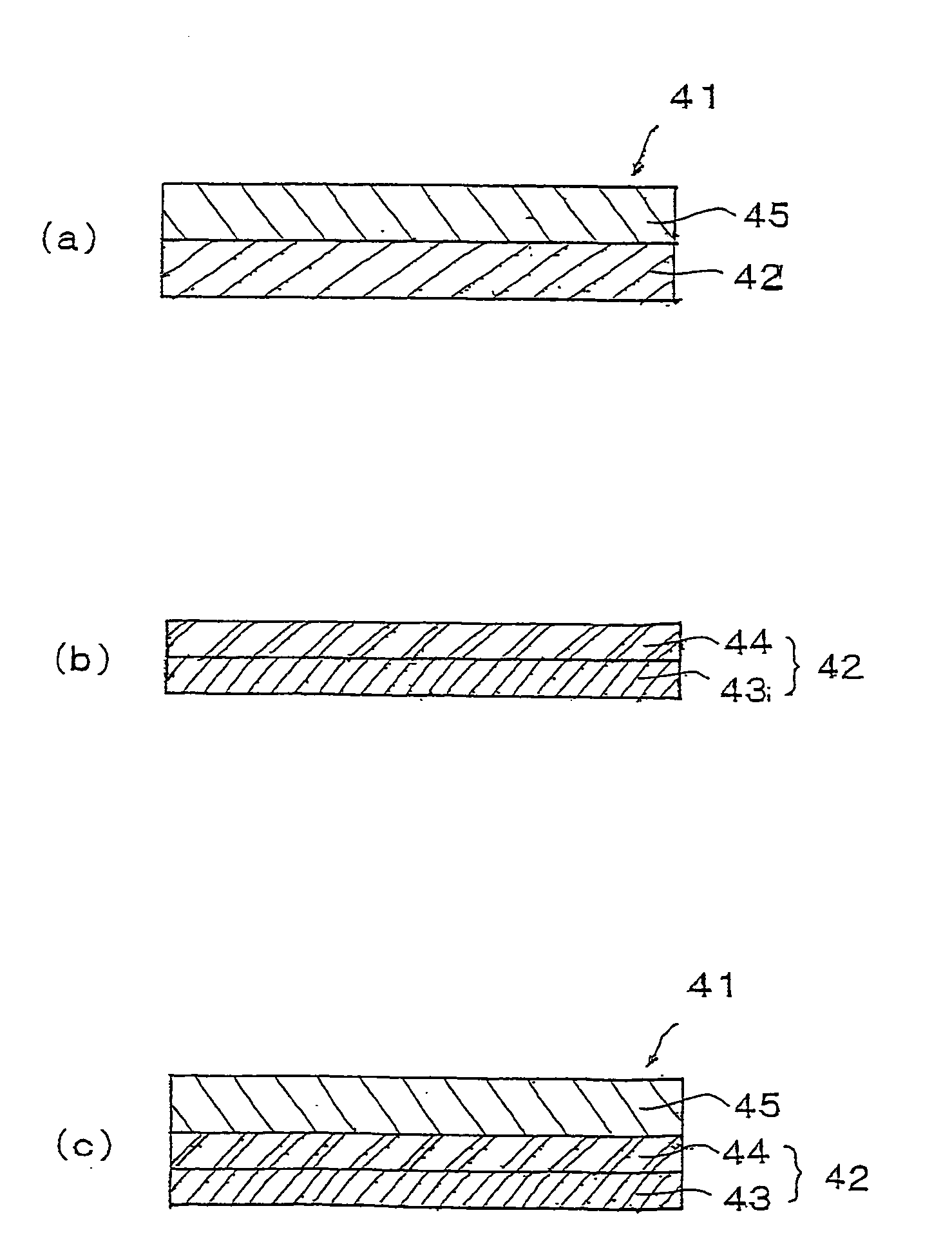
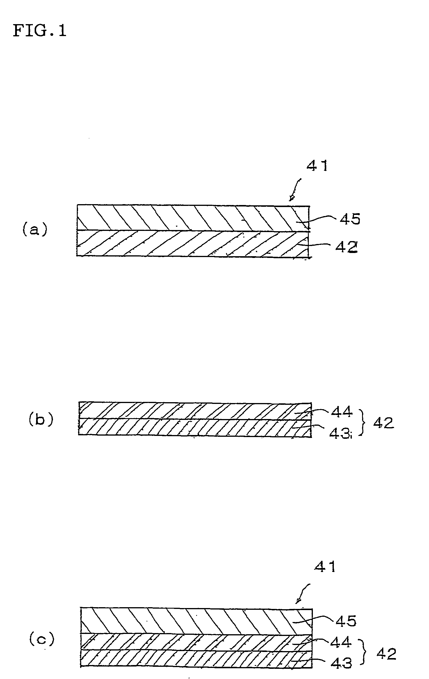
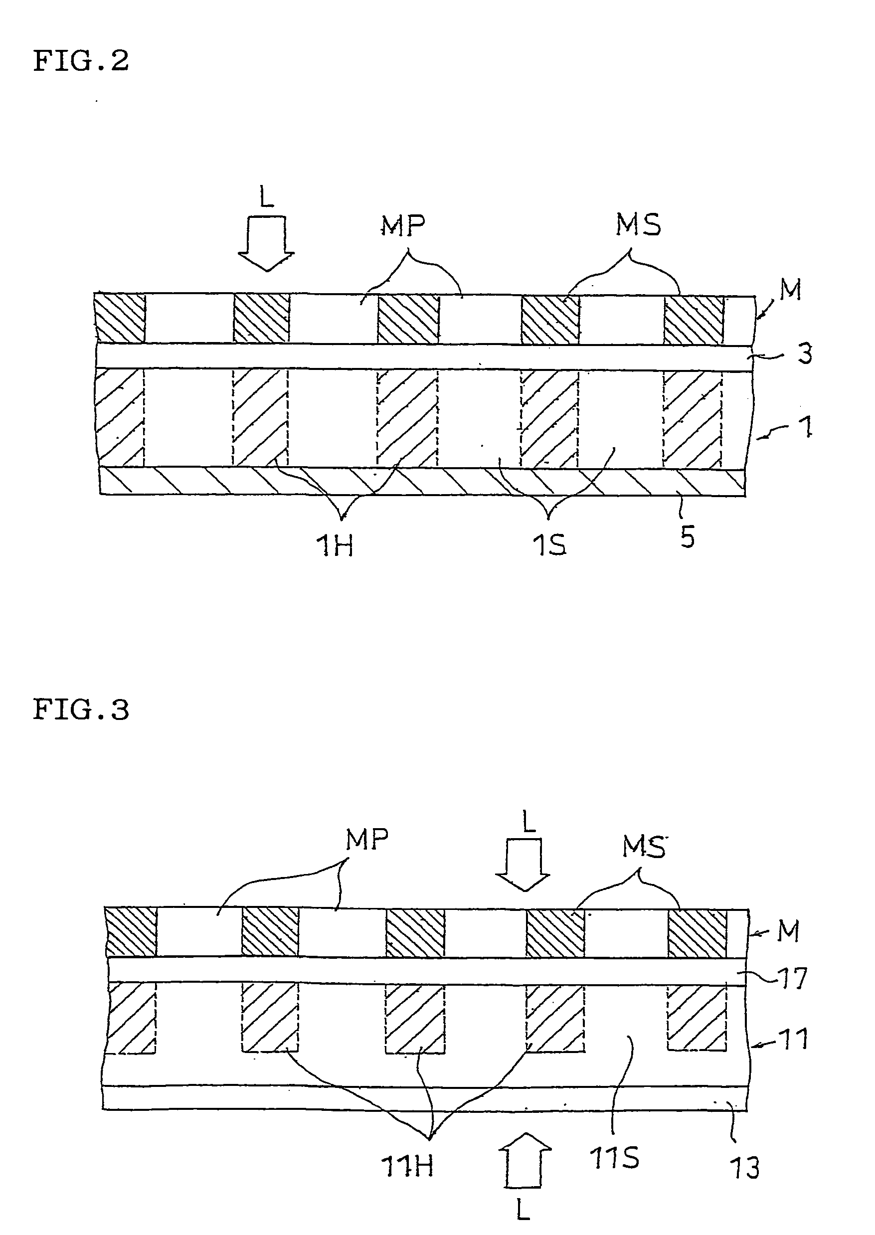
Image

Examples
example 1
Example 1-1
[0300] 125 g epoxy acrylate (EX5000, methyl ethyl ketone solvent, solids content 80%, manufactured by Kyoeisha Chemical Co., Ltd.), 1 g benzyl dimethyl ketal and 0.1 g hydroquinone methyl ether were mixed under stirring by a kneader, and the solvent was removed under reduced pressure, whereby a solid photosetting composition was obtained. This composition was sandwiched between films and pressed at 10 atmospheric pressure with a pressing machine at 100.degree. C., to give a sheet molding of 2 mm in thickness. This sheet molding was irradiated with UV rays, and the other side with a mask film having a desired pattern drawn thereon was irradiated with UV rays, and after the films were removed, the sheet was developed by rubbing with a brush in a toluene solvent. The sheet was dried at 60.degree. C. for 30 minutes to give a polishing pad.
[0301] This polishing pad was evaluated for polishing by the polishing evaluation method A.
example 1-2
[0302] 200 g polyurethane resin (Vylon UR-1400, toluene / methyl ethyl ketone (1 / 1 by weight) solvent, solids content 30%, manufactured by Toyo Boseki Co., Ltd.), 40 g trimethylol propane trimethacrylate, 1 g benzyldimethyl ketal and 0.1 g hydroquinone methyl ether were mixed under stirring by a kneader, and the solvent was removed, whereby a solid photosetting composition was obtained. This composition was sandwiched between films and pressed at 10 atmospheric pressure with a pressing machine at 100.degree. C., to give a sheet molding of 2 mm in thickness. This sheet molding was irradiated with UV rays for a predetermined time, and the other side with a mask film having a desired pattern drawn thereon was irradiated with UV rays, and after the films were removed, the sheet was developed. The sheet was dried at 60.degree. C. for 30 minutes to give a polishing pad. Its subsequent evaluation was carried out in the same manner as in Example 1-1. =
example 1-3
[0303] 145 g urethane acrylate (UF503LN, methyl ethyl ketone solvent, solids content 70%, manufactured by Kyoeisha chemical Co., Ltd.), 1 g benzyl dimethyl ketal and 0.1 g hydroquinone methyl ether were mixed under stirring by a kneader, and the solvent was removed, whereby a solid photosetting composition was obtained. This composition was sandwiched between films and pressed at 10 atmospheric pressure with a pressing machine at 100.degree. C., to give a sheet molding of 2 mm in thickness. This sheet molding was irradiated with UV rays for a predetermined time, and the other side with a mask film having a desired pattern drawn thereon was irradiated with UV rays, and after the films were removed, the sheet was developed. The sheet was dried at 60.degree. C. for 30 minutes to give a polishing pad. Its subsequent evaluation was carried out in the same manner as in Example 1-1.
Example 1-4
[0304] 258 g polyurethane resin (Vylon UR-8400, toluene / methyl ethyl ketone (1 / 1 by weight) solven...
PUM
 Abstract
Description
Claims
Application Information