
Wafer dicing/die bonding sheet

a technology of die bonding and waxing, which is applied in the direction of heat-activated film/foil adhesives, film/foil adhesives, synthetic resin layered products, etc., can solve the problems of loss of bonding force, insufficient polyimide resins to mitigate thermal stress, and insufficient cure properties

Active Publication Date: 2004-06-03
SHIN ETSU CHEM IND CO LTD
View PDF6 Cites 39 Cited by
  • Summary
  • Abstract
  • Description
  • Claims
  • Application Information

AI Technical Summary

Benefits of technology

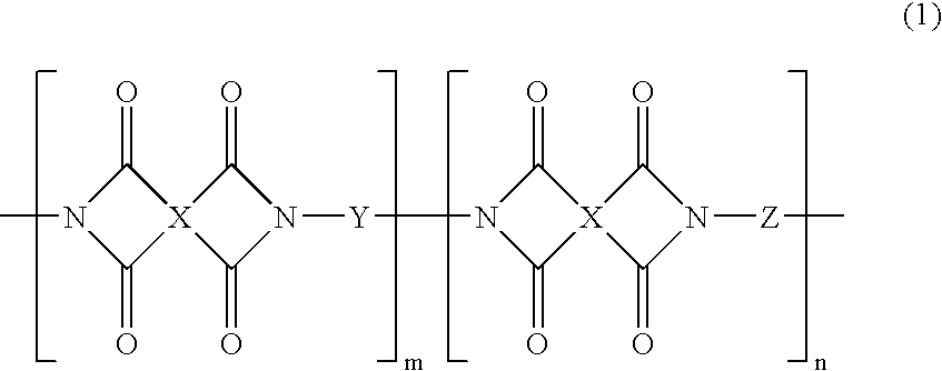
[0010] The present invention is directed to a wafer dicing / die bonding sheet comprising a backing member, an adhesive layer formed thereon, and a protective member for protecting the adhesive layer. It has been found that when the adhesive layer is made of an adhesive composition comprising a phenolic hydroxyl radical-bearing polyimide resin, an epoxy resin, and an epoxy resin curing agent, the resulting wafer dicing / die bonding sheet readily adheres to a wafer at room temperature or under heat and pressure, can be used as the dicing tape in the dicing step, is kept adhered to the rear side of a chip as a die bonding agent after the dicing step, and allows the chip to be directly bonded to a lead frame. Since this composition has improved heat resistance, adhesive properties and a low modulus of elasticity, the cured adhesive layer is effective for minimizing the warpage of the chip after die bonding, and substantially prevents the package from cracking and separating during solder reflow. The dicing / die bonding sheet improves the reliability of a semiconductor device fabricated using the same.

Problems solved by technology

On account of a high glass transition temperature (Tg) and a high modulus of elasticity, the polyimide resins are insufficient to mitigate the thermal stress between bonded substrates of semiconductor parts.
Most prior art polyimide base adhesives are thermoplastic and thus problematic in that they lose a bonding force at high temperatures as encountered when advanced lead-free solders are used.
Since phenolic hydroxyl radicals are present at sterically packed positions, their reaction with the epoxy resin is hindered, resulting in insufficient cured properties and insufficient bond strength at high temperatures.
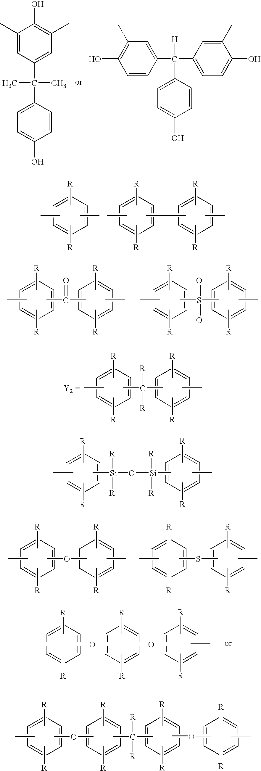
Too low a proportion of phenolic hydroxyl radical-containing amine component (ii) may lead to less substrate adhesion whereas too high may lead to an increased modulus of elasticity and a loss of flexibility.
Too low a proportion of diaminosiloxane component (iii) may achieve less flexibility-imparting effect whereas too high may lead to an increased moisture permeability and poor heat resistance.
The gelled product has an ester bond structure and so it undergoes hydrolysis under hot humid conditions to decompose into lower molecular weights, causing a loss of humidity-resistant reliability.
To prevent esterification reaction by the reaction of phenolic hydroxyl radicals with acid anhydride radicals, capping phenolic hydroxyl radicals with protective radicals is possible, but is not necessarily recommended in the industrial application because of an increased process expense and an increased cost of protective radical reactant.
Too less crosslinking points with the epoxy resin are undesirable because adhesion and heat resistance become poor.
If too less epoxy radicals are available, adhesion to an adherend becomes insufficient.
If too much epoxy radicals are available, the excess of epoxy resin increases the modulus of elasticity, which is inconvenient to form a flexible adhesive sheet.
A total amount of less than 10 pbw fails to achieve sufficient crosslinking to provide adhesion whereas a total amount in excess of 300 pbw renders the adhesive layer hard and brittle.
Less than 0.1 pbw of the silane coupling agent may fail to enhance the adhesion whereas the adhesion enhancement achieved with more than 5 pbw may not be so satisfactory relative to the cost.

Method used


Image

  • Wafer dicing/die bonding sheet
  • Wafer dicing/die bonding sheet
  • Wafer dicing/die bonding sheet

Examples


synthesis example 1

[0062] A 1-liter separable flask equipped with a 25-ml water metering receiver coupled to a reflux condenser through a cock, a thermometer and a stirrer was charged with 44.03 parts of a diaminosiloxane (linear dimethylpolysiloxane blocked with a .gamma.-aminopropyldimethylsiloxy radical at each end of the molecular chain, KF-8010 by Shin-Etsu Chemical Co., Ltd.) and 100 parts of cyclohexanone as a reaction solvent. By stirring at 80.degree. C., the diaminosiloxane was dispersed. A solution of 38.72 parts of 6FDA (2,2-bis(3,4-dicarboxyphenyl)hexafluoropropane) as an acid anhydride in 100 parts of cyclohexanone was added dropwise to the dispersion. The solution was stirred for 8 hours at 80.degree. C. for reaction, thereby synthesizing an acid anhydride-rich amic acid oligomer.

[0063] Next, a 1-liter separable flask equipped with a 25-ml water metering receiver coupled to a reflux condenser through a cock, a thermometer and a stirrer was charged with 17.25 parts of a phenolic hydroxyl...

synthesis example 2

[0065] In a flask equipped with a stirrer, thermometer and nitrogen purge line, 29.42 g (0.10 mol) of 3,3',4,4'-biphenyltetracarboxylic acid dianhydride, 7.46 g (0.03 mol) of 1,3-bis(3-aminopropyl)-1,1,3,3-tetramet-hyldisiloxane, and 28.73 g (0.07 mol) of 2,2-bis(4-(4-aminophenoxy)phenyl)-propane in 196.8 g of N-methyl-2-pyrrolidone were reacted at room temperature for 12 hours, yielding a polyamic acid solution. Toluene, 30 g, was added to the polyamic acid solution, and reaction effected at 200.degree. C. for 3 hours. It was confirmed that a predetermined amount of water collected in the water metering receiver and the outflow of water ceased. While the water metering receiver was freed of the effluent, the toluene was removed completely at 160.degree. C., yielding a polyimide resin solution. At the end of reaction, the solvent was distilled off from the solution, and vacuum drying yielded the polyimide resin.

[0066] The infrared absorption spectrum of the polyimide resin was measu...

example 1

[0067] In 600 parts of cyclohexanone were dissolved 100 parts of the polyimide resin obtained in Synthesis Example 1, 71.3 parts of o-cresol novolac epoxy resin EOCN1020 (by Nippon Kayaku Co., Ltd., epoxy equivalent 220 g / Eq), 27.7 parts of a phenol novolac resin TD2131 (Dainippon Ink & Chemicals, Inc., phenolic hydroxyl equivalent 110 g / Eq), 1 part of triphenylphosphine TPP (Hokko Chemical Co., Ltd.) as the curing catalyst and 1 part of 3-glycidoxypropyltrimethoxy-silane as the silane coupling agent. There was obtained an adhesive composition varnish.


PUM

PropertyMeasurementUnit
molar ratioaaaaaaaaaa
temperatureaaaaaaaaaa

Abstract

In a wafer dicing / die bonding sheet comprising a backing member, an adhesive layer, and a protective member, the adhesive layer is made of an adhesive composition comprising a phenolic hydroxyl radical-bearing polyimide resin, an epoxy resin, and an epoxy resin curing agent, the ratio of the total weight of the epoxy resin and the epoxy resin curing agent to the weight of the polyimide resin being from 0.1:1 to 3:1. Due to heat resistance, improved adhesive properties and a low modulus of elasticity, the wafer dicing / die bonding sheet is effective for reducing the warpage of a chip after die bonding.

Description

[0001] 1. Field of the Invention[0002] This invention relates to a wafer dicing / die bonding sheet for use in the dicing of silicon wafers and the bonding of chips to lead frames.[0003] 2. Background Art[0004] In the prior art, semiconductor devices are generally manufactured by securing a large diameter silicon wafer to a dicing tape, dicing the wafer into semiconductor chips, peeling and removing the chips from the dicing tape, and bonding an individual chip to a lead frame with a curable liquid adhesive.[0005] For simplifying the process and preventing contamination of semiconductor chips with fluid ingredient from the liquid adhesive, there is recently a need for a dicing / die bonding sheet in the form of a pressure-sensitive adhesive sheet that serves as both the pressure-sensitive adhesive layer of dicing tape and the die bonding agent. The dicing / die bonding sheet needs to develop an adhesive (or retentive) force to withstand the dicing operation and to adhere to the chip being...

Claims


Application Information

Patent Timeline
Patent Type & Authority Applications(United States)
IPC IPC(8): C09J177/00B32B7/12C08L63/00C08L79/08C09J7/22C09J7/35C09J163/00C09J179/08H01L21/52H01L21/58H01L21/68
CPCB32B7/12H01L2924/10253C08L79/08C09J7/0242C09J163/00C09J179/08C09J2203/326C09J2463/00C09J2479/08H01L21/6836H01L24/27H01L24/29H01L24/83H01L2221/68327H01L2224/274H01L2224/2919H01L2224/83191H01L2224/8385H01L2924/01004H01L2924/01005H01L2924/01015H01L2924/01027H01L2924/01039H01L2924/01047H01L2924/01077H01L2924/01082H01L2924/07802H01L2924/14H01L2924/19042H01L2924/3511C08L63/00H01L2924/00013Y10S525/928H01L2224/29101H01L2924/0665H01L2924/014H01L2224/29H01L2224/29298H01L2924/01006H01L2924/01019H01L2924/01023H01L2924/01024H01L2924/01033H01L2924/01045C08L2666/20C08L2666/22H01L2924/07025H01L2924/00H01L2924/00012H01L2924/3512H01L2224/29099H01L2224/29199H01L2224/29299H01L2224/2929H01L2924/15787C09J7/35C09J7/22Y10T428/31511Y10T428/31721Y10T428/31515Y10T428/31663C09J177/00
Inventor SHIOBARA, TOSHIOICHIROKU, NOBUHIROAKIBA, HIDEKIYOSHINO, MASACHIKA
Owner SHIN ETSU CHEM IND CO LTD
Learn More