
Simultaneously achieving circular symmetry and diminishing effects of optical defects and deviations during real time use of optical devices

a technology of optical devices and circular symmetry, which is applied in the field of optical systems, devices, tools, instruments, etc., to achieve the effect of reducing distortion and astigmatism, improving the quality of optical devices or systems, and reducing asymmetrical aberrations

Inactive Publication Date: 2005-01-27
SYMMETRITECH
View PDF17 Cites 8 Cited by
  • Summary
  • Abstract
  • Description
  • Claims
  • Application Information

AI Technical Summary

Benefits of technology

[0053] It is therefore an object of the present invention to provide a method for simultaneously achieving circular symmetry and diminishing effects of optical defects and deviations during real time viewing and projecting by optical devices.
[0066] Additionally, with respect to manufacturing optical devices and systems, implementation of the present invention reduces production time and effort required to achieve tight design specifications of an optical device or system, resulting in lower production costs and shorter delivery times. Enables acceptance of components and elements of an optical device or system that otherwise would be rejected during testing processes, resulting in reduced manufacturing costs and time. Removes the risk of optical device or system failure due to effects of shipment and / or environmental conditions.

Problems solved by technology

An overlay metrology tool, however, inherently introduces its own error into the overlay measurement.
This error has two components, known as the accuracy error, and the repeatability or reproducibility error.
Accuracy error, also referred to as Tool Induced Shift (TIS), directly arises from distortions and aberrations in the optics of the overlay metrology tool.
Repeatability error may arise from several factors, optics being one of them.
The stepper must produce an overlay better than or within the overlay budget, however, the overlay metrology tool must in turn, produce a total error less than about one tenth of that.
This tight margin of total error, especially the TIS component, translates to extremely strict requirements on the optical quality of an overlay metrology tool.
Although features and objects, such as landscape and buildings, viewed by such optical equipment are relatively large, the large distances from which they are viewed result in minute details appearing in a viewed image, which can be thought of as scaling to similar conditions and dimensions involved in micro-lithography.
Such optical elements cannot be rotated without affecting or changing the optical behavior of light or radiation interacting with or passing through the optical element.
An optical device, featuring a single lens 44 or 46, is extremely performance limited and of poor quality.
With regard to interaction of light with matter, the laws of physics imply that, even if all basic components, such as lenses and mirrors, of an optical device or system are perfectly designed, manufactured, and assembled, the optical device or system as a whole would still deviate from ideal desired optical behavior.
The problem with designing a more complex optical device, with the goal of achieving a better theoretical optical behavior, is that as the number of optical elements featured in an optical device grows, so does the probability for introduction of additional optical defects and deviations into the optical device, originating from the manufacturing and assembly of additional optical elements.
No matter how much care and cost go into manufacturing individual optical elements of an optical device, such as glass lenses and mirrors, there are always found varying degrees of optical defects such as impurities, imperfections, and / or blemishes.
Moreover, every polished glass surface has some degree of deviation from the required shape, known as form errors.
In addition, individual lenses are usually covered with a coating material, such as anti-reflective coating, which introduces additional form errors and blemishes.
Performing quality control inspection and testing on an optical device typically requires elaborate and time-consuming procedures, and even with sophisticated testing equipment and instrumentation, it is impossible to detect all defects.
Manufacturing costs and time involved in rejecting finished products failing specifications are extremely high.
The above described optical defects and deviations cause an optical device to deviate from its designed optical behavior, resulting in the occurrence of various aberrations and disturbances, such as coma and astigmatism, during real time application of the optical device.
However, this practice has the negative effect of reducing optical resolution of the optical device, as optical resolution is proportional to the numerical aperture (NA) of the optical device, decreasing with physical size of the aperture.
Stopping down a lens assembly may be quite acceptable for recreational or educational applications of optical devices, however, typically it is highly undesirable for applications in leading edge technologies such as semiconductor fabrication.
During shipment, the optical device may be exposed to mechanical shock, severe pressure change if shipped by air, and severe temperature changes.
Thus, even following a comprehensive, costly, and quality controlled cycle of design, manufacture, and assembly, an optical device may still feature defects and / or deviations at the time of application by an end-user.
Unfortunately, this is never the case, since the components of an optical device, in general, and of an optical assembly or lens assembly, including optical elements such as lenses and / or mirrors, in particular, can never be perfectly manufactured, and assembled, for producing a perfectly functioning optical device.
Moreover, the presence of optical defects and / or deviations from ideal symmetry is likely to increase with increasing sophistication in the design of an optical device, as an increasing number of optical elements, peripheral structures, and peripheral mechanisms inherently leads to the presence of additional optical defects and deviations in the optical device.
Impurities or blemishes are randomly scattered throughout the raw material, preventing the manufacture of a uniform glass or plastic, and hence preventing the achievement of circular symmetry of the optical element, and consequently, of the optical device.
However, such polished surfaces usually feature random locations of irregularities.
In addition, in a polished lens, there always exist form errors or shape irregularities, including symmetric and / or asymmetric form errors.
The common practice of plating an optical element with a coating material, such as anti-reflective coating, introduces yet additional blemishes and form errors into the optical element.
The presence of these form errors and irregularities prevent the polished lens, and consequently, the optical device, from featuring a high degree of circular symmetry.
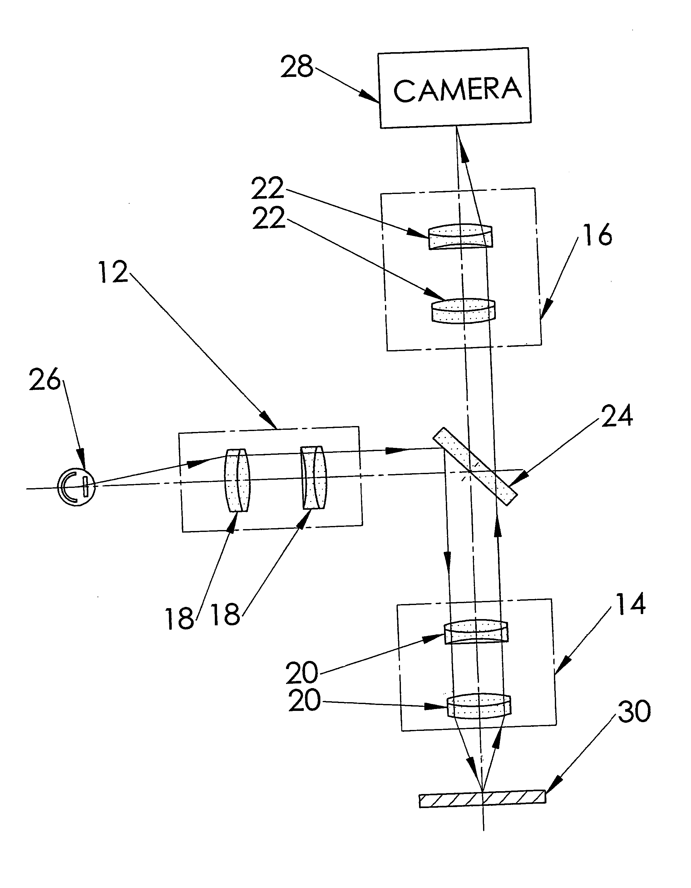
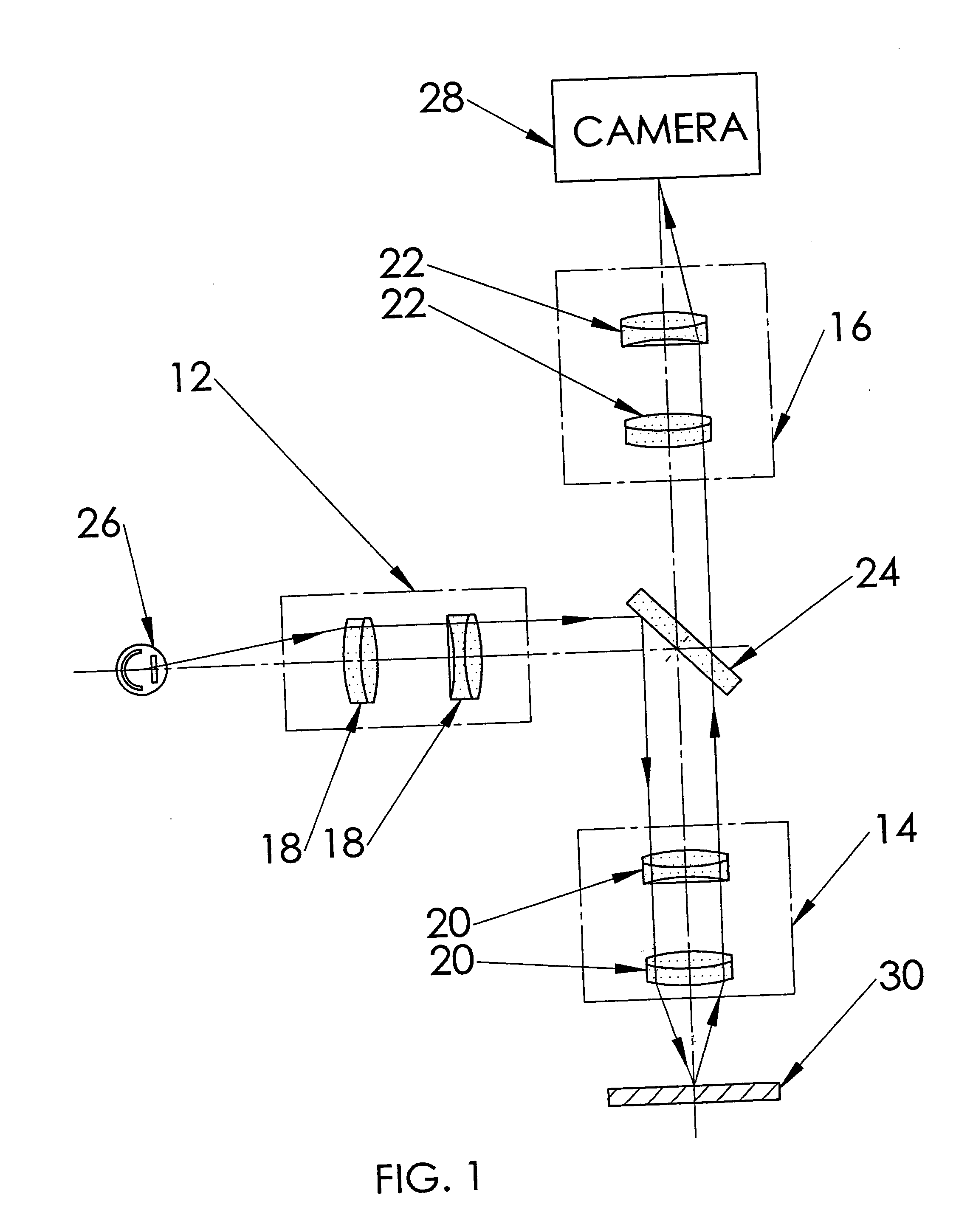
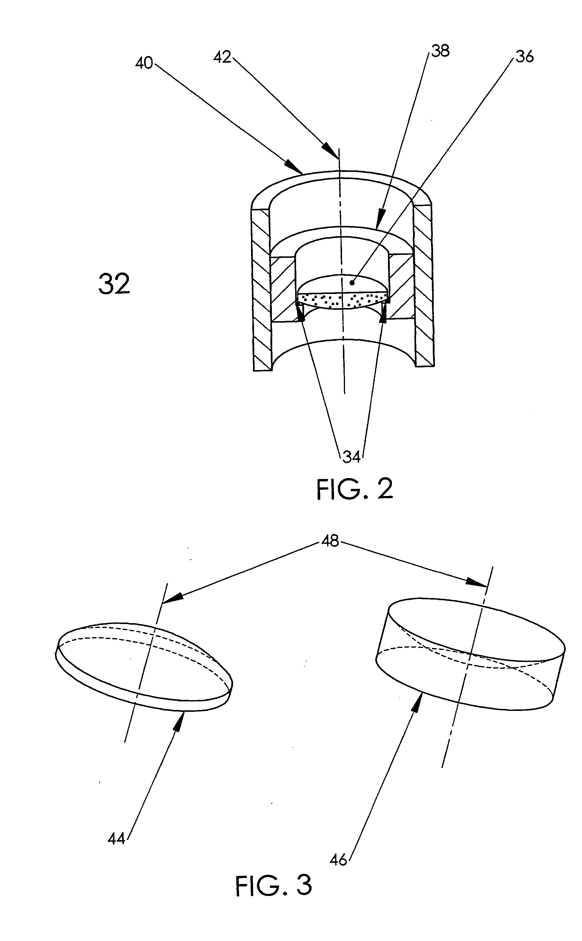
However, as described and shown in FIGS. 2 and 3, some combination of horizontal and / or angular deviations are inevitably present in the assembled optical device, thereby preventing the entire optical device, and not only the separate optical elements, from featuring circular symmetry.
For example, optical devices and systems including a peripheral mechanism such as a radiation source, in general, or a light source, in particular, may be subject to further non-uniformities introduced by the source.
In general, it is desirable, but practically impossible, to obtain a source that produces radiation of uniform intensity over the entire field of view, or field of projection.
Integration occurring during exposure time is usually considered in the art as very undesirable.
When taking a picture, for example, too long of an exposure time, or, equivalently, too slow of an aperture speed, can cause blurring or smearing in images of an object.
In the Riggs disclosure, separate optical elements are mounted and separately rotated with different velocities, which places substantial mechanical complexity on such an apparatus.
Moreover, the fact that individual optical elements need to be separately handled, prohibits the use of proven, inexpensive and readily available mass produced off-the-shelf sealed optical assemblies such as objectives, which ordinarily cannot be taken apart for facilitating approach to the individual optical elements.
The method thus forces the design, manufacturing, and assembly of totally new and unique optical assemblies, again placing substantial constraints on the practicality of the method.
Additional limitations apparent in the Riggs disclosure are that the method uses a series of separate exposures at time and rotation intervals, which is limited in its effect compared to a single prolonged exposure which better ‘smears’ and diminishes the effect of optical disturbances, and there is not provided a means for aligning the mechanical axis of rotation of the individual lens mounts with the optical axis of the lens being rotated.
A general significant limitation of other prior art methods, is that they deal with effects of optical defects and deviations at the time of manufacture, assembly, and / or set-up of an optical device, for example, by translating, rotating, and aligning optical elements and / or assemblies of the optical device to an optimum configuration and performance level, immediately followed by permanently fixing, such as by cementing, the optical elements and / or assemblies, prior to release of the optical device to an end-user, or prior to use of the optical device by the end-user.
This procedure is very limited, since simple movements of one optical element usually cannot compensate for complex disturbances originating in other optical elements of the same optical device.
Any additional rotation would degrade the performance of the projection unit.
The method is limited by not providing means for correcting various types of optical disturbances, and may even lead to introduction of new systematic disturbances.
As described above, even after applying such devices and methods for diminishing effects of optical defects and deviations, there still remains high likelihood of the presence of optical defects and deviations of the optical device by the time an end-user includes the optical device in an application.
In addition, following repetitive or modified use of an initially optimally configured and performing optical device, optical defects and deviations are expected to appear, thereby limiting further application of the optical device.

Method used


Image

  • Simultaneously achieving circular symmetry and diminishing effects of optical defects and deviations during real time use of optical devices
  • Simultaneously achieving circular symmetry and diminishing effects of optical defects and deviations during real time use of optical devices
  • Simultaneously achieving circular symmetry and diminishing effects of optical defects and deviations during real time use of optical devices

Examples


first embodiment

[0095] In this first embodiment of the method, Step 2 of rotating at least one optical part of the optical device causes spreading and blurring, about the rotation axis of the at least one optical part of the optical device, of optical defects and deviations present in the at least one optical part of the optical device. This results in diminishing the effects of optical defects and deviations during real time viewing or projecting by the rotated at least one optical part of the optical device, while an image that is either viewed or projected by the optical device remains intact.

[0096] As previously discussed and illustrated in FIG. 5, an optical device, such as a lens assembly, can feature at least one optical element having its optical axis perfectly aligned and coinciding with the common mechanical axis of the tube of the lens assembly, while simultaneously featuring at least one optical element having its optical axis misaligned with the common mechanical axis of the tube of th...

second embodiment

[0104] In this second embodiment of the method, Step 2 of aligning the optical axis of the at least one optical part of the optical device, achieves circular symmetry of the at least one optical part of the optical device, according to the alignment procedure described and illustrated in FIG. 8. Combined with Step 3 of rotating the at least one optical part of the optical device, causes circularly symmetrical spreading and blurring about the rotation axis of optical defects and deviations present in the at least one optical part of the optical device. This results in additionally diminishing the effects of optical defects and deviations present in the at least one optical part of the optical device, compared to rotating without aligning the at least one optical part of the optical device, during real time viewing or projecting, while an image that is either viewed or projected by the optical device remains intact.

[0105] In the second embodiment of the method, Step 2 of aligning the ...


PUM

PropertyMeasurementUnit
sizeaaaaaaaaaa
circular symmetryaaaaaaaaaa
elasticaaaaaaaaaa

Abstract

A method for simultaneously achieving circular symmetry and diminishing effects of optical defects and deviations during real time use of optical devices, and, a corresponding device and system for implementing the method thereof. The method features rotating an entire optical device, rotating at least one optical part of an entire optical device such as an optical assembly or an optical element during real time viewing or projecting by the optical device, in order to spread and blur the optical defects and deviations present in the at least one optical part of the optical device. In a first embodiment of the method, an optical rotation device is activated and controlled for rotating at least one optical part of an optical device during real time use of a viewing or projecting optical device. In a second embodiment of the method, there is included a step for aligning the optical axis of the at least one optical part of the optical device with respect to the rotation axis. In a first, simple, yet practical, embodiment of an optical rotation device for rotating the at least one optical part of the optical device, there are provided means and mechanisms for manual alignment during real time use of an optical device, whereas, in a second, more advanced, embodiment of an optical rotation device for effecting the rotation of the optical part of the optical device, there are provided means and mechanisms for highly accurate and automatic aligning of the optical axis of the optical part of the optical device with the rotation axis, thereby simultaneously achieving a high level of circular symmetry with respect to the optical part of the optical device, and significant diminishment of optical defects and deviations in at least one optical part of the optical device.

Description

FIELD AND BACKGROUND OF THE INVENTION [0001] The present invention relates to optical systems, devices, tools, and instruments, and to other systems having optical components and, more particularly, to a method for simultaneously achieving circular symmetry and diminishing effects of optical defects and deviations during real time use of optical devices, and, a corresponding device and system for implementing the method thereof. [0002] In contrast to common recreational and educational uses of optical viewing or projection devices and systems, the field of semiconductor device fabrication requires the technology of design, manufacture, and implementation of such devices and systems to be pushed to the utmost limit. Here, semiconductor devices are fabricated on silicon wafers, where a single wafer, capable of containing multiple semiconductor devices, is made up of a multiple of overlaid layers, in sequence, one on top of the other. Photolithography is an initial stage in the process...

Claims


Application Information

Patent Timeline
Patent Type & Authority Applications(United States)
IPC IPC(8): G02BG02B7/00G02B7/02G02B26/08G02B27/00G02B27/18G02B27/22G03F7/20H01L21/027
CPCG02B26/0875G02B26/0883G03F7/70825G03F7/70258G02B27/0025G02B26/00
Inventor YANOWITZ, SHIMON
Owner SYMMETRITECH
Learn More