
Method of manufacturing a semiconductor device

Inactive Publication Date: 2005-02-24
SEMICON ENERGY LAB CO LTD
View PDF25 Cites 10 Cited by
  • Summary
  • Abstract
  • Description
  • Claims
  • Application Information

AI Technical Summary

Benefits of technology

Electrons are accelerated in the θ direction to collide with gas molecules in the induction filed E, thereby producing plasma. Since the direction of the induction field E is the θ direction, the probability that charged particles collide with an inner wall of a reaction chamber and the substrate 505 to lose energy is small. Further, the magnetic field B hardly affects the portion below the antenna coil 502, and thus, a high density plasma region that is expanded in a flat plate shape is produced. Then, the high frequency power applied to the lower electrode 506 is adjusted, whereby the plasma density and the bias voltage applied to the substrate 505 can be independently controlled. Further, the frequency of the high frequency power to be applied can be changed in accordance with a substance to be etched.
In order to generate high density plasma with the ICP system, the high frequency current J that flows through the antenna coil needs to be flown at a low loss, and the inductance needs to be lowered. In view of this point, a method in which the antenna coil is divided is effective. FIG. 4B is a schematic diagram showing such a structure. A portion consisting of a plurality of spiral coils 510 is arranged on a quartz substrate 509, and is connected to a first high frequency power source 512 through a matching box 511. In this case, when the length of one coil is set to an integral multiple of ¼ of a high frequency wavelength, a standing wave occurs in the coil portion, and a peak value of the generated voltage can be increased.
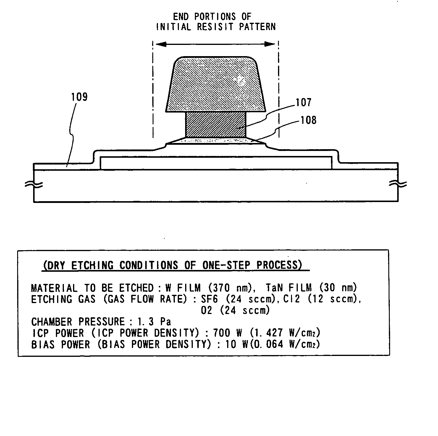
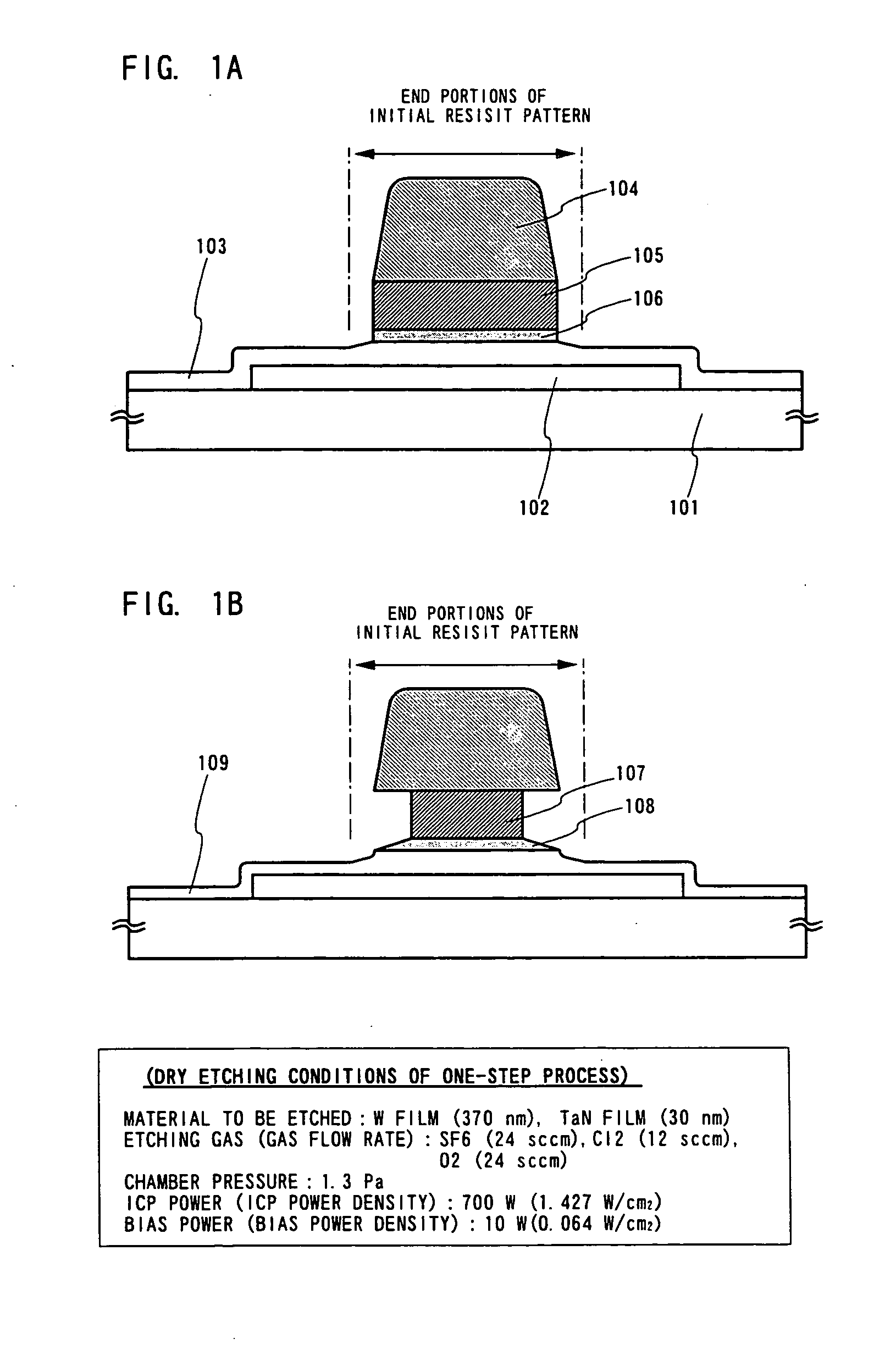
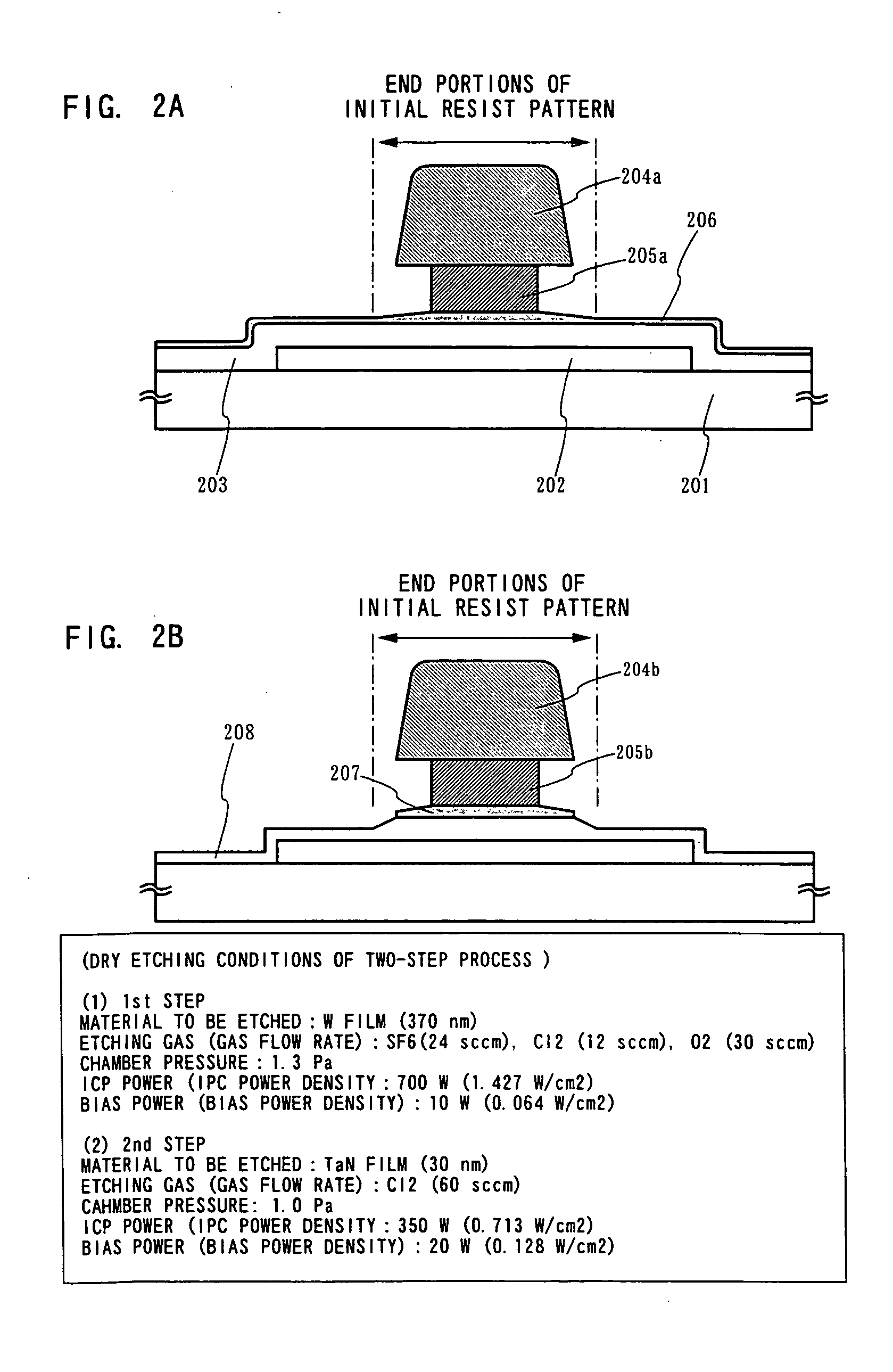
Note that the silicon oxide film is used as the gate insulating film here, and is the most preferable one. However, the present invention is not limited to this. As described above, it is considered that the silicon oxide film is exposed in over etching, and that oxygen emitted from the silicon oxide film causes side etching of the W film. Therefore, it is considered that the same effect can be obtained with a film other than the silicon oxide film as long as the film is an oxide film.
According to the present invention structured as described above, the gate electrode of the semiconductor device the circuit of which is configured by a plurality of TFTs including the GOLD structure TFT can be processed by the dry etching process consisting of one step or two steps. Accordingly, there can be solved the problems in the prior art in the dry etching process, that is, reduction in throughput of the dry etching process, rise of the process cost that follows consumption amount increase of etching gas, and further, reduction of yield of a semiconductor device which follows complication of the dry etching process.

Problems solved by technology

These have been problems in terms of reliability.
Thus, the LDD structure has a defect that a drain current decreases.
Further, there has been the problem of a deterioration mode peculiar to the LDD in which: a high electric field region exists just under the side wall; impact ionization becomes maximum there; hot electrons are implanted into the side wall; and thus, the low concentration impurity region (n− region or p− region) is depleted, and the resistance is further increased.

Method used


Image

  • Method of manufacturing a semiconductor device
  • Method of manufacturing a semiconductor device
  • Method of manufacturing a semiconductor device

Examples


embodiment mode 1

In this embodiment mode, a description will be given of manufacturing steps of a semiconductor display device having TFTs of an LDD structure and a GOLD structure on a glass substrate as a transparent insulating substrate with reference to FIGS. 8A to 10B. Note that, a specific circuit configuration is as follows: a pixel TFT is composed using an LDD structure excellent in low OFF current characteristics and an n-channel or a p-channel driver circuit is composed using a GOLD structure high in resistance to hot carriers.

First, on a glass substrate 601 as a transparent insulating substrate which is formed in a square shape with a side being 12.5 cm, an amorphous silicon film having a thickness of 20 to 200 nm, preferably 30 to 70 nm, is deposited by a plasma CVD method or a reduced pressure CVD method. In this embodiment mode, the amorphous silicon film having a thickness of 53 nm is deposited. Thereafter, a polycrystalline silicon film is formed with a thickness of 50 nm through h...

embodiment mode 2

In this embodiment mode, a description will be given of manufacturing steps of a semiconductor display device having TFTs of an LDD structure and a GOLD structure, which are different from Embodiment Mode 1 with reference to FIGS. 11A to 12D. Specific circuit configuration in this case is similar to that in Embodiment Mode 1. Note that, manufacturing steps shown in FIGS. 11A and 11B are basically the same as those in Embodiment Mode 1 (FIGS. 8A and 8B) and thus are shown in a simple manner.

First, on a glass substrate 801 as a transparent insulating substrate which is formed in a square shape with a side being 12.5 cm, an island-like semiconductor layer 802 made of a polycrystalline silicon film (crystalline silicon film being substitutable therefor, which is formed utilizing a catalytic element) having a thickness of 50 nm is formed. A gate insulating film 803a made of a silicon oxide film (silicon oxynitride film being substitutable therefor) having a thickness of 100 nm is then...

embodiment 1

In this embodiment, a specific description will be given of a manufacturing method for an active matrix liquid crystal display device using the present invention with reference to FIGS. 13A to 18B. Note that this embodiment basically employs the same manufacturing method as in Embodiment Mode 1 except that a crystalline silicon film crystallized using a catalytic element is adapted for the semiconductor layer as an active layer of the TFT instead of using the general polycrystalline silicon film.

First, on a glass substrate 1001 are deposited by a plasma CVD method silicon oxynitride films 1002a and 1002b as a first layer with a thickness of 50 nm and a second layer with a thickness of 100 nm, respectively, with different composition ratios, so as to constitute a base film 1002. Note that, the glass substrate 1001 used in this case may be made of quartz glass, barium borosilicate glass, aluminoborosilicate glass, etc. Next, on the base film 1002 (1002a and 1002b), an amorphous sil...


PUM


Abstract

A semiconductor device is provided which is constituted by semiconductor devices including a thin film transistor with a GOLD structure, the GOLD structure thin film transistor being such that: a semiconductor layer, a gate insulating film, and a gate electrode are formed in lamination from the side closer to a substrate; the gate electrode is constituted of a first-layer gate electrode and a second-layer gate electrode shorter in the size than the first-layer gate electrode; the first-layer gate electrode corresponding to the region exposed from the second-layer gate electrode is formed into a tapered shape so as to be thinner toward the end portion; a first impurity region is formed in the semiconductor layer corresponding to the region with the tapered shape; and a second impurity region having the same conductivity as the first impurity region is formed in the semiconductor layer corresponding to the outside of the first-layer gate electrode, which is characterized in that a dry etching process consisting of one step or two steps is applied to the formation of the gate electrode.

Description

BACKGROUND OF THE INVENTION 1. Field of the Invention The present invention relates to a semiconductor device and a method of manufacturing the same, and particularly to a thin film transistor (hereinafter referred to as TFT) with a GOLD (abbreviated form of “gate-overlapped-LDD”) structure and a method of manufacturing the same. Note that the semiconductor device in this specification indicates semiconductor devices in general the circuit of which is configured by semiconductor devices including a TFT with a GOLD structure. For example, semiconductor display devices such as an active matrix liquid crystal display device and an organic EL (abbreviated form of “electro-luminescence”) display device are included in the category of the semiconductor device. 2. Description of the Related Art In semiconductor display devices, such as an active matrix liquid crystal display device and an organic EL display device, the circuit of which is configured by TFTs on a transparent insulating ...

Claims


Application Information

Patent Timeline
IPC IPC(8): H01L21/336H01L21/77H01L21/84H01L27/12H01L29/423H01L29/49H01L29/786
CPCH01L27/1214H01L29/42384H01L29/4908H01L2029/7863H01L29/78621H01L29/78627H01L29/78675H01L29/66757H01L27/127
Inventor OKAMOTO, SATORU
Owner SEMICON ENERGY LAB CO LTD
Features
  • Generate Ideas
  • Intellectual Property
  • Life Sciences
  • Materials
  • Tech Scout
  • Unparalleled Data Quality
  • Higher Quality Content
  • 60% Fewer Hallucinations
Learn More