Thin film transistor and method for production thereof

Inactive Publication Date: 2005-03-31
SONY CORP
View PDF2 Cites 20 Cited by
  • Summary
  • Abstract
  • Description
  • Claims
  • Application Information

AI Technical Summary

Benefits of technology

It is an object of the present invention to provide a thin film transistor and a method for production thereof. The thin film transistor works at a higher speed owing to polycrystalline semiconductor film, permits its driving current to be increased, and exhibits uniform characteristic properties. The manufacturing method is practicable with a less number of steps and is applicable to larger substrates than before.
As mentioned above, the present invention provides a method for producing a thin film transistor. This manufacturing method is characterized in forming the active layer and the source-drain layer by the reactive heat CVD process. Therefore, it eliminates the steps for crystallizing the semiconductor thin film and introducing impurities into the source-drain layer, and it gives rise to a polycrystalline semiconductor thin film which works at a higher speed. The stacked thin film transistor obtained in this manner permits the driving current, or ON current, to be increased. With this manufacturing method, it is possible to simplify production process, reduce production cost, and eliminate quality variation due to crystallization. Without steps for crystallization and doping, it is possible to form uniform thin film transistors on a larger substrate. This, in turn, helps realize a large-sized display unit with thin film transistors.
The stacked thin film transistor obtained by the above-mentioned manufacturing method is characterized in that the active layer and the source-drain layer are formed from a polycrystalline semiconductor thin film deposited by the reactive heat CVD process. Therefore, it works at a higher speed. Moreover, the source and drain regions are formed such that they overlap the gate electrode in a specific manner. This helps increase the driving current.

Problems solved by technology

However, it suffers the disadvantage of requiring an additional step for recrystallization and resulting in TFT's varying in properties due to fluctuating laser energy.
Unfortunately, these apparatus are applicable only to substrates no larger than approximately 730 by 920 mm2 (or substrates of the fourth generation).
This is a primary factor that makes it difficult to realize large-sized displays.

Method used


Image

  • Thin film transistor and method for production thereof
  • Thin film transistor and method for production thereof
  • Thin film transistor and method for production thereof

Examples


first embodiment

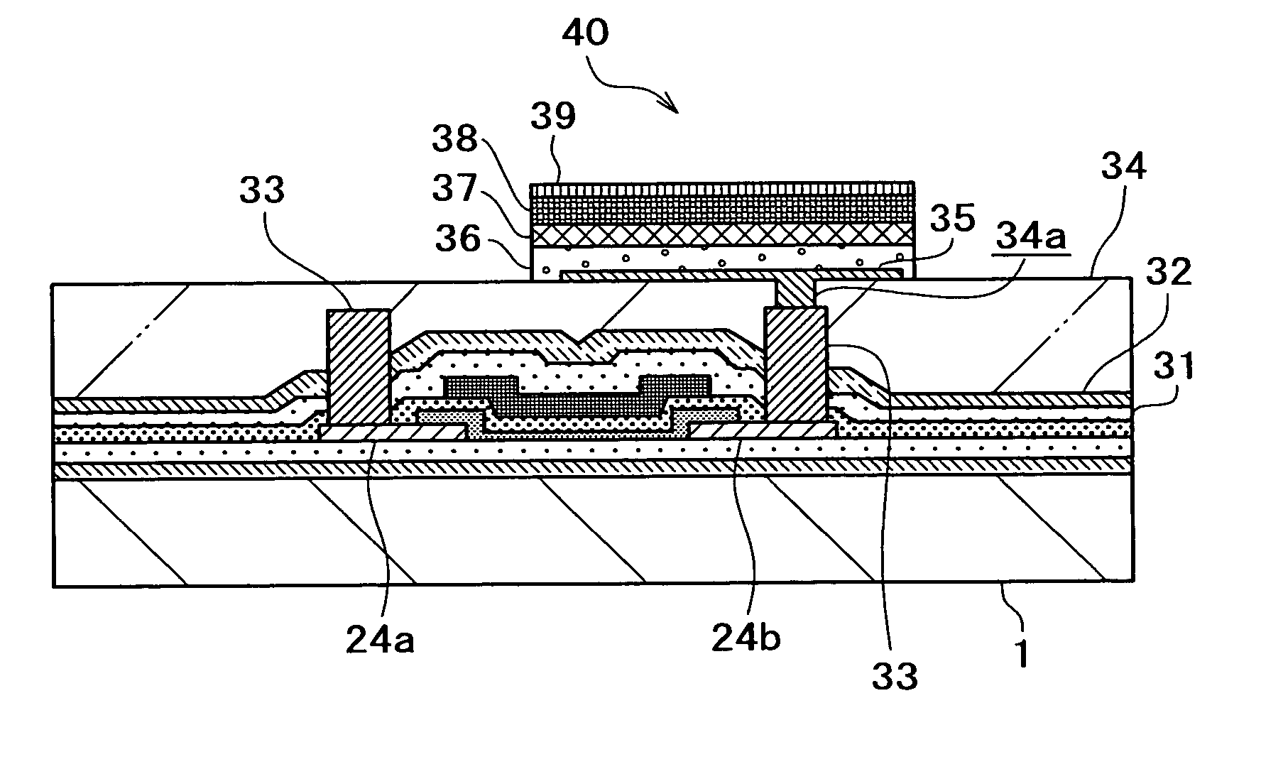
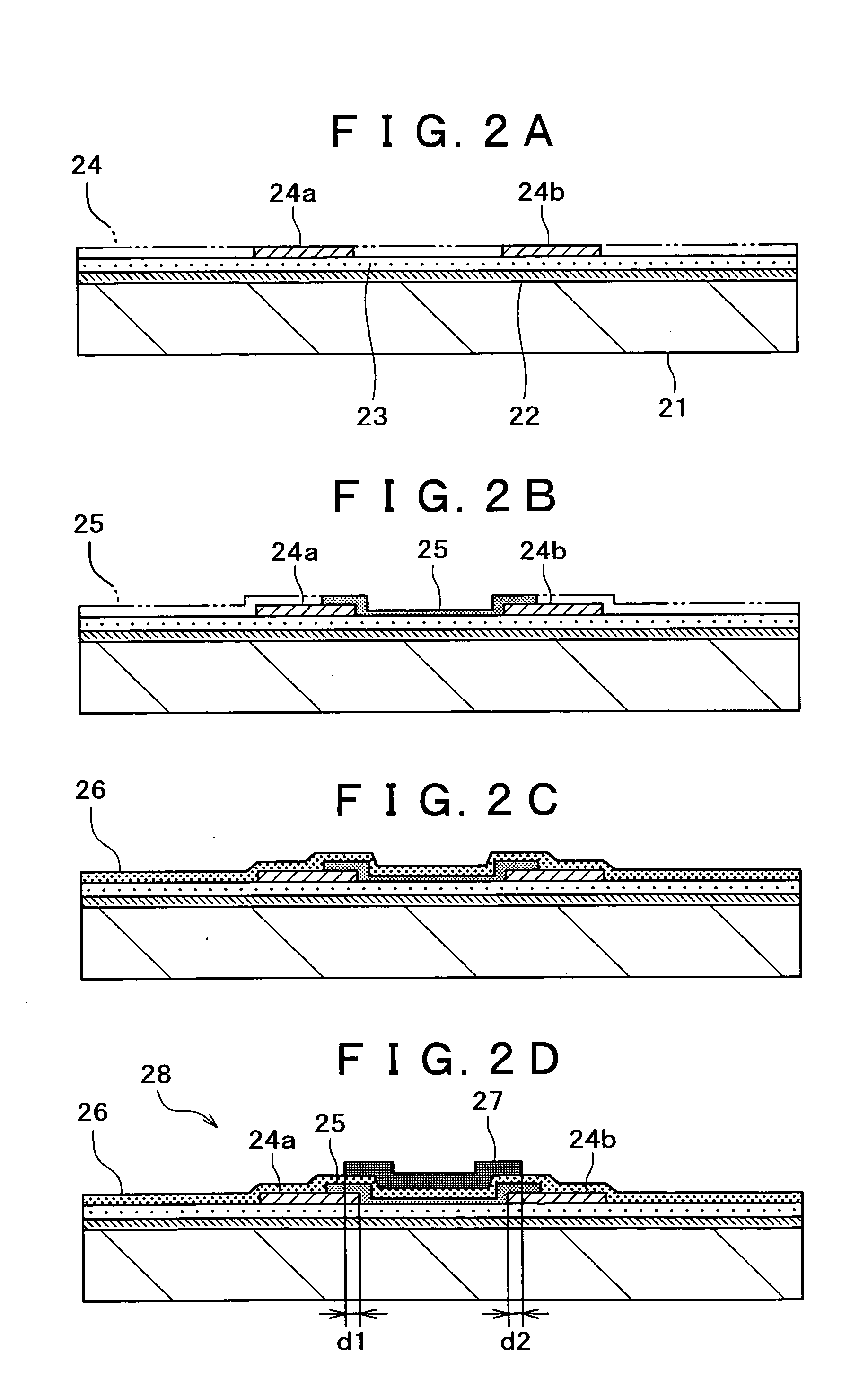
FIGS. 2A to 4B are sectional views which illustrate the method for producing thin film transistors in the first embodiment. The following is concerned with the method for producing a stacked TFT of top gate type as a thin film semiconductor device. The following is also concerned with the method for producing a display device with said stacked TFT's.

The first step is to prepare an insulating substrate 21 as shown in FIG. 2A. The substrate 21 may be AN635 or AN100 (from Asahi Glass) or Codel 1737 or Eagle 2000 (from Corning) or the like.

On the substrate 21 are sequentially formed a silicon nitride (SiNx) film 22 as a buffer layer and a silicon oxide film (SiOx) 23, which have a thickness ranging from about 50 to 400 nm.

Then, on the silicon oxide film 23 is formed by the reactive heat CVD process a source-drain layer 24 from polycrystalline silicon or polycrystalline silicon-germanium containing an n-type (or p-type) impurity. The source-drain layer 24 may be a single-layer film...

second embodiment

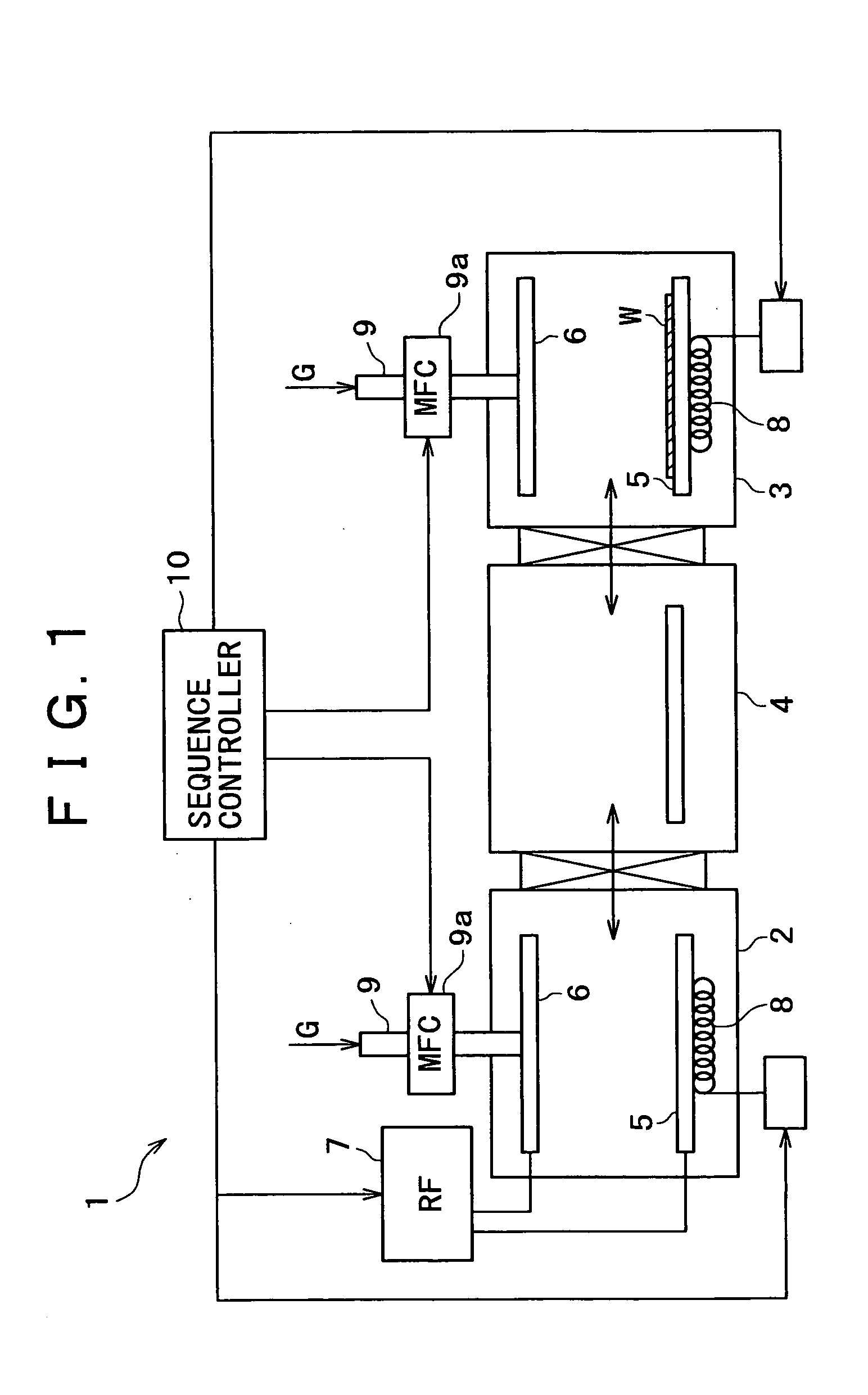
Sectional views of FIGS. 5 and 6 illustrate the method for producing thin film transistors in the second embodiment. The following is concerned with the method for producing a stacked TFT of bottom gate type as a thin film semiconductor device. The following is also concerned with the method for producing a display device with said stacked TFT's.

First, as shown in FIG. 5A, an insulating substrate 51 is coated with a conductive film of 50 to 250 nm thick of tantalum (Ta), molybdenum (Mo), tungsten (W), chromium (Cr), copper (Cu), or an alloy thereof, in the same way as in the first embodiment. Then, this conductive film is made into gate electrodes 52 by patterning.

Subsequently, as shown in FIG. 5B, a silicon nitride film 53a of 30 to 50 nm thick and a silicon oxide film 53b of 50 to 200 nm thick are sequentially formed by plasma CVD, atmospheric CVD, or reduced pressure CVD. The resulting laminate film is made into a gate insulating film 53.

Then, an active layer 54 of impurit...


PUM


Abstract

The production method of the thin film transistor according to the present invention involves the reactive heat CVD process to form the active layer and the source-drain layer. This offers the advantage of eliminating additional steps to crystallize the semiconductor thin film. The resulting stacked thin film transistor is composed of originally crystalline semiconductor thin films. Having the active layer and the source-drain layer formed from crystalline semiconductor thin film, the stacked thin film transistor has a faster working speed than the one formed from amorphous semiconductor thin film. Another advantage of eliminating steps for crystallization is uniform quality which would otherwise be adversely affected by crystallization. In addition, the fact that the source-drain layer is formed from a previously doped crystalline semiconductor thin film means that there is no need for any step to introduce impurities after film formation.

Description

BACKGROUND OF THE INVENTION The present invention relates to a thin film transistor and a method for production thereof. The thin film transistor is of the stacked type which is made of polycrystalline silicon. It finds use as an element to drive the liquid crystal display or organic electroluminescence (EL for short hereinafter) of active matrix type. A display device of active matrix type is provided with thin film transistors (TFT) as driver elements. TFT's are classed into that of stacked type and that of planar structure. The former has an active layer separate from the source-drain region, and the latter has a channel section of the same semiconductor layer as the source-drain region. The TFT of stacked type offers the advantage of requiring less masks in its manufacturing process, which is mentioned in the following. FIG. 9 is a sectional view showing a stacked TFT of bottom gate type. This TFT is produced as follows. The process starts with sequentially forming on a substr...

Claims


Application Information

Patent Timeline
IPC IPC(8): H01L51/50H01L21/336H01L21/77H01L21/84H01L27/12H01L29/786H05B33/10
CPCH01L27/1214H01L29/66757H01L29/66765H01L29/78696H01L29/78675H01L29/78678H01L29/78618H01L27/127H01L27/1274
Inventor KUNII, MASAFUMI
Owner SONY CORP
Why Eureka
Try Eureka