Group-III nitride semiconductor device

a technology of nitride and semiconductors, applied in the field of groupiii nitride semiconductor layers and groupiii nitride semiconductor devices, can solve the problems of nitride semiconductors, damage to the active layer of the device, and difficulty in realizing a high yield of the device over a large area, so as to reduce the leakage of current, and reduce the density of dislocations.

Inactive Publication Date: 2005-04-07
RENESAS ELECTRONICS CORP
View PDF10 Cites 297 Cited by
  • Summary
  • Abstract
  • Description
  • Claims
  • Application Information

AI Technical Summary

Benefits of technology

[0064] The intentional introduction of oxygen may provide the following two advantageous effects. The first advantageous effect is to realize a desired highly planer surface morphology. As described above, the nitride-based amorphous layer is partially etched, prior to the crystallization of the partially etched nitride-based amorphous layer. The presence of oxygen atoms over the surface region or in the upper region of the partially etched nitride-based amorphous layer contributes to suppress an undesired mass-transport of one or more kinds of atoms of the partially etched nitride-based amorphous layer. The suppression to the undesired mass-transport prevents non-flatness of the surface of the crystallized nitride-based compound semiconductor layer. Namely, the suppression to the undesired mass-transport realizes an island-free planarized surface of the crystallized nitride-based compound semiconductor layer. The desired island-free planarized surface of the crystallized nitride-based compound semiconductor layer may be transferred to the surface of the additional crystal layer over the crystallized nitride-based compound semiconductor layer, whereby a desired highly planarized surface morphology may be obtained.
[0065] The absence of oxygen atoms over the surface region or in the upper region of the partially etched nitride-based amorphous layer may allow an undesired mass-transport of one or more kinds of atoms of the partially etched nitride-based amorphous layer. The allowance of the undesired mass-transport may cause non-flatness of the surface of the crystallized nitride-based compound semiconductor layer. Namely, the allowance of the undesired mass-transport may result in an undesired island-like non-planarized surface of the crystallized nitride-based compound semiconductor layer. The undesired island-like non-planarized surface of the crystallized nitride-based compound semiconductor layer may be transferred to the surface of the additional crystal layer over the crystallized nitride-based compound semiconductor layer, whereby any undesired non-planarized surface morphology may be obtained.
[0066] The second advantageous effect is to realize a reduction in leakage of current. As described above, the crystallized nitride-based compound semiconductor layer has a relatively high density of dislocations such as edge dislocations upon the crystallization process. The relatively high density of dislocations allows leak current to flow along the dislocations. However, oxygen atoms present over the surface region or in the upper region of the partially etched nitride-based amorphous layer are likely to be selectively localized to the dislocations in the crystallization process, whereby the dislocations become electrically inactive which reduces the leakage of current along the dislocations. This makes the nitride-based compound semiconductor crystal layer suitable as current confinement layer.
[0067] In a typical example, the oxygen-introduced region of the partially etched nitride-based compound semiconductor crystal layer may have an oxygen concentration of at least 1E18 cm−3.
[0068] In one typical example, the partially etched nitride-based compound semiconductor crystal layer with the opening may be applicable to a current confinement layer in a laser diode. Namely, the first aspect of the present invention may advantageously be applicable to the formations of any electron devices having a current confinement layer, for example, laser diodes.
[0069] In another typical example, the partially etched nitride-based compound semiconductor crystal layer with the opening may be applicable to electrode contact layers, for example, source / drain contact layers, on which source and drain electrodes are provided in a field effect transistor. Namely, the first aspect of the present invention may advantageously be applicable to the formations of any field effect transistors.

Problems solved by technology

The Group-III nitride semiconductors are, however, not suitable in micro-processability or etching-controllability, while improvement or increase in micro-processability or etching-controllability of the Group-III nitride semiconductors are essential for realizing desirable high performances of the Group-III nitride semiconductor device.
For those reasons, it is difficult to realize a high yield of the devices over a large area.
Further, charge particles generated in the etching process may provide a damage to the active layer of the device.
This p-n junction causes a junction capacitance which may further cause a deterioration in high frequency performance.
This means a difficulty of the crystal growth process for growing the undoped nitride semiconductor layer over the n-doped nitride semiconductor layer.
The first issue is concerned with a possible formation of crack which may be formed by differences in both lattice constant and thermal expansion coefficient between AlN and other nitride semiconductors such as AlGaN, GaN and InGaN.
Accordingly, it is difficult to suppress cracks completely.
The crack in the AlN layer not only does render the current confinement layer dysfunctional in current confinement but also does cause the laser diode chip to be broken.
The second issue with the AlN current confinement layer is concerned with a difficulty in selective removal of the AlN current confinement layer.
It is difficult to realize a desired selective etching of AlN and either GaN, AlGaN or GaN by utilizing the chlorine-based dry etching process because of physical sputtering effect in the dry etching process.
It is also difficult for the chlorine-based dry etching process to suppress undesired variation in etching depth of the nitride material due to variation in etching conditions.
Namely, it is difficult for the chlorine-based dry etching process to realize a desired high etching-controllability of the nitride material.
Therefore, the chlorine-based dry etching process has a difficulty to achieve a desired high yield and is likely to cause a problem with an etching-damage.
It is also disclosed by M. S. Minsky in Applied Physics Letter 68 (1996) 1531-1533 that these alkali etchants etch not only AlN but also GaN with an imperfect etching-selectivity and further cause an undesired deterioration in after-etching-morphology of the etched portion.
The deterioration in the morphology causes a deterioration in crystal quality or crystal imperfection of re-grown layer.
This is the significant problem.
As far as this method is concerned, the coverage of side walls of the mask by the AlN layer makes it difficult to carry out the intended left-off method.
The limitation in the thickness of the deposited AlN layer provides a limitation to the desired increase in the withstand voltage of the device, and also allows an undesired increase in the leakage of current, resulting in an insufficient current confinement.
A further problem is that residual impurities of the lift-off mask may cause a deterioration in the device.
Particularly if the mask material is silicon oxide, for example, SiO2 or SiOx, then it is difficult to completely remove residual Si, for which reason it is likely that a pile-up of Si is formed over a re-growth interface of the cladding layer.
The pile-up of Si may cause a deterioration of electric characteristics of the device.

Method used


Image

  • Group-III nitride semiconductor device
  • Group-III nitride semiconductor device
  • Group-III nitride semiconductor device

Examples


example 1

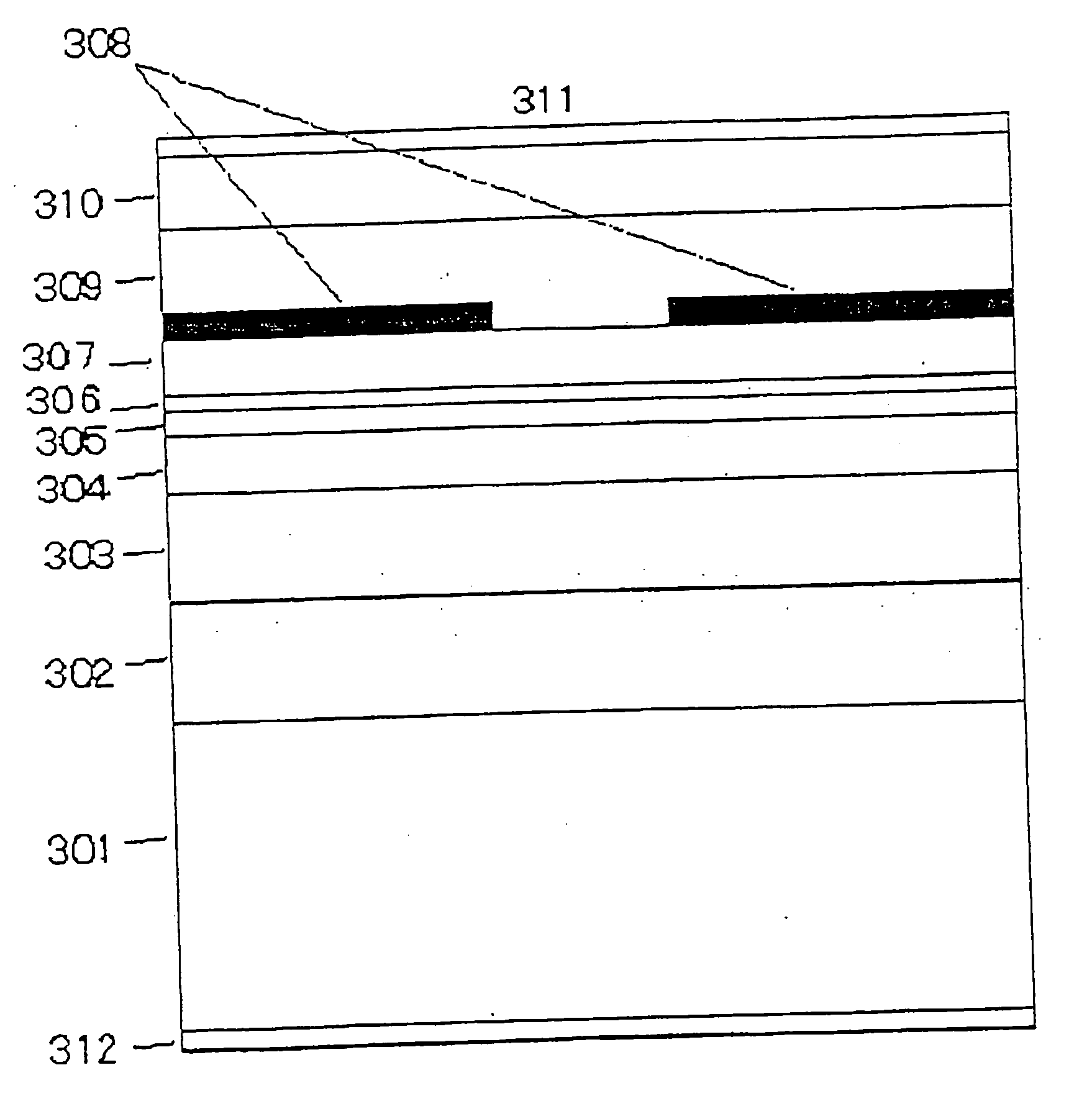
[0139] The following example 1 is involved in the above-described embodiment shown in FIG. 3. An n-type GaN layer with a (0001)-plane and a thickness of 250 micrometers was grown over a sapphire substrate by use of a facet-initiated epitaxial lateral overgrowth method which is disclosed by A. Usui et al. in Japan of Journal Applied Physics 36 (1997) L899. After the growth of the n-type GaN layer, the substrate was then subjected to a cooling process in which the n-type GaN layer was peeled from the sapphire substrate due to a significant difference in thermal expansion coefficient between GaN crystal and sapphire crystal, whereby the substrate was a free-standing GaN substrate with a thickness of 200 micrometers.

[0140] For forming a device structure, a low pressure metal organic vapor phase epitaxy system was used for epitaxial growth under a low pressure of 300 hPa. A mixture gas of hydrogen and nitrogen was used as a carrier gas. A trimethyl gallium gas (TMG), a trimethyl aluminu...

example 2

[0170] The “multi-layered structure growth processes” were carried out in the same manners as in Example 1 to form the lamination structure of the above n-type GaN buffer layer, the above n-type AlGaN cladding layer, the above n-type GaN guide layer, and the above InGaN multiple quantum well active layer, the above p-type GaN guide layer and the amorphous AlN layer for a current confinement layer. The growth of the amorphous AlN layer was carried out at the substrate temperature of 400° C. The wafer was then loaded into a normal pressure anneal reactor, and 1 SLM of oxygen and 4 SLM of nitrogen were supplied for causing a surface oxidation of the wafer at 400° C. for 20 minutes.

[0171] Subsequently, the “stripe-shaped opening formation process” was then carried out in the same manner as in Example 1 for forming the above stripe-shaped opening in the amorphous AlN layer.

[0172] Subsequently, the “multi-layered structure re-growth processes” were then carried out in the same manner as...

example 3

[0196] An amorphous GaN layer was grown on a single crystal GaN layer at a temperature of 350° C. before the amorphous GaN layer was then subjected to a selective wet etching, by use of the single crystal GaN layer as an etching stopper and of a hot etchant of 95° C. which contains phosphate and sulfate at 1:1 ratio. The etching rate was that etching by 0.1 micrometer depth takes a time in the range of 20-40 minutes. The wet etching process was terminated when the surface of the single crystal GaN layer underlying the amorphous GaN layer, whereby a “Sample-D” was obtained.

[0197] Similarly, another amorphous GaN layer was grown on another single crystal GaN layer at a different temperature of 400° C. before the amorphous GaN layer was then subjected to a selective wet etching, by use of the single crystal GaN layer as an etching stopper and of the same hot etchant of 95° C. which contains phosphate and sulfate at 1:1 ratio. The etching rate was that etching by 0.1 micrometer depth t...


PUM

PropertyMeasurementUnit
dislocation densityaaaaaaaaaa
temperatureaaaaaaaaaa

Abstract

A method of forming a partially etched nitride-based compound semiconductor crystal layer includes the following steps. A non-crystal layer of a nitride-based compound semiconductor is formed. At least a part of the non-crystal layer is then etched to form a partially etched non-crystal layer before the partially etched non-crystal layer is crystallized to form a partially etched nitride-based compound semiconductor crystal layer.

Description

CROSS REFERENCE TO RELATED APPLICATIONS [0001] This application is a division of co-pending application Ser. No. 10 / 231,163, filed on Aug. 30, 2002, the entire contents of which are hereby incorporated by reference.BACKGROUND OF THE INVENTION [0002] 1. Field of the Invention [0003] The present invention relates to a method for forming a Group-III nitride semiconductor layer and a Group-III nitride semiconductor device. [0004] All of patents, patent applications, patent publications, scientific articles and the like, which will hereinafter be cited or identified in the present application, will, hereby, be incorporated by references in their entirety in order to describe more fully the state of the art, to which the present invention pertains. [0005] 2. Description of the Related Art [0006] Group-III nitride semiconductors have relatively large forbidden band gaps and allow a direct transition between conduction and valence bands, for which reason applications of the Group-III nitrid...

Claims


Application Information

Patent Timeline
Patent Type & Authority Applications(United States)
IPC IPC(8): B82Y10/00H01L21/205B82Y20/00B82Y40/00H01L21/20H01L21/306H01L21/338H01L29/778H01L29/812H01L33/14H01S5/22H01S5/323H01S5/343
CPCH01L21/02389H01L21/02458H01L21/02505H01L21/0254H01S2304/00H01L21/30612H01L33/145H01S5/2206H01S5/32341H01L21/0262
Inventor SASAOKA, CHIAKI
Owner RENESAS ELECTRONICS CORP
Why Eureka
Try Eureka