
A structure of a lateral diffusion mos transistor in widespread use as a power control device

a technology of lateral diffusion mos and transistor, which is applied in the direction of transistors, semiconductor devices, electrical equipment, etc., can solve the problems of limited downsizing of power control systems and large structures that are still required, and achieve the effects of reducing the on-resistance of the device, reducing the size of the power control system, and increasing the curren

Inactive Publication Date: 2005-05-05
LAPIS SEMICON CO LTD
View PDF4 Cites 15 Cited by
  • Summary
  • Abstract
  • Description
  • Claims
  • Application Information

AI Technical Summary

Benefits of technology

[0011] With an LDMOS that is the semiconductor device of the above-described configuration, since current flows along the gate electrode formed in the respective trench cavities, inside the substrate, it is possible to secure a channel corresponding to a depth of the trench cavities on the outer side faces of the trench cavities. Furthermore, since a current between a source and drain is dependent on the depth of the trench cavities, a device area can be developed without taking into account a gate length and gate width on a plane as with the case of a conventional LDMOS transistor, thereby enabling a large current to be controlled. Furthermore, since the source electrode and drain electrode are formed in the trench cavities, respectively, paths of current flowing through conduction layers in the substrate become shorter, and the current can directly reach the electrodes, so that on-resistance of the device can be further reduced. Further, the invention is applicable to either a PMOS or the NMOS.
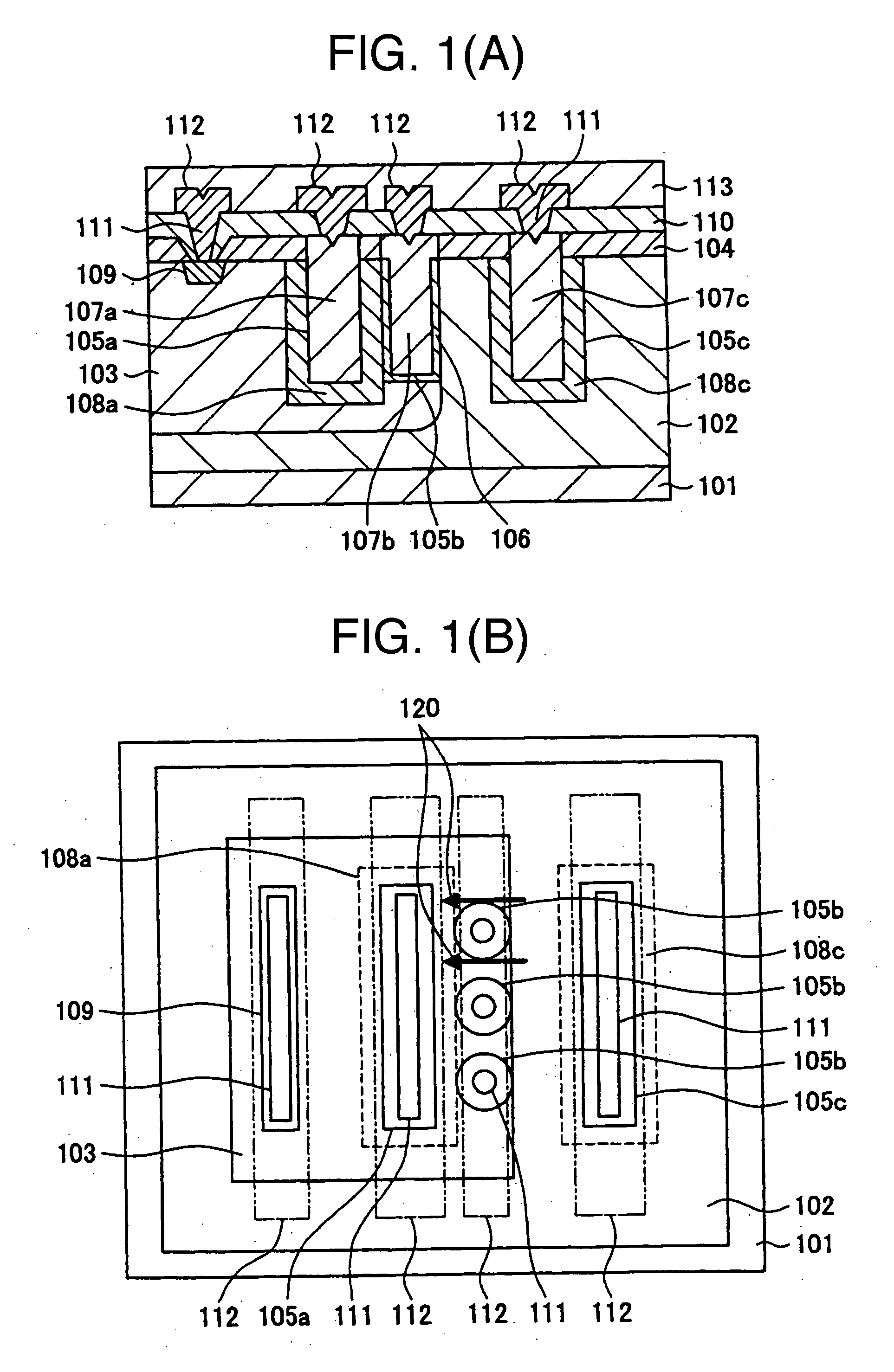
[0012] Herein, a plurality of the trench cavities for the gate electrodes are preferably disposed in a line in the direction of a channel width. In this case, the direction of the channel width refers to a direction normal, or perpendicular to a direction in which a current flows from the drain electrode to the source electrode. Thus, a channel serving as a current path is induced on respective side faces of the plurality of the trench cavities, so that larger current can be controlled without increasing the device area. Further, it is desirable to form the trench cavities for the gate electrodes substantially in the shape of a column, thereby preventing malfunction due to electric field concentration, and so forth.
[0013] Further, the trench cavities for the gate electrodes preferably have a depth equal to a depth of the first heavily doped region for reduction of the on-resistance. Furthermore, an impurity concentration of the layer of the first conductivity is preferably rendered higher than that of the layer of the second conductivity forming the drain electrode, thereby extending a depletion layer toward the drain side, so that a short channel effect can be prevented, and a higher voltage resistance of the drain can be attained.
[0014] The structure of the present invention can be applied to a SOI substrate provided with an insulating oxide film layer formed underneath the layer of the second conductivity type. In this case, the thickness of the layer of the first conductivity type formed in the layer of the second conductivity type so as to be smaller than that of the layer of the second conductivity type as in the case of a common bulk substrate can be rendered the same as the thickness of the layer of the second conductivity type. With the SOI structure adopted, occurrence of a parasitic bipolar transistor can be prevented and parasitic capacitance can be reduced, thereby preventing malfunction of operation and enabling high-speed operation and low current consumption to be achieved, so that the device can obtain more excellent characteristics.

Problems solved by technology

With a semiconductor device for power control, however, a structure with a large area is still required in effecting power control, which has been the main stumbling block for implementing downsizing of LSI chips.
Accordingly, with the conventional LDMOS structure, there has been a limitation to downsizing of a power control system.

Method used


Image

  • A structure of a lateral diffusion mos transistor in widespread use as a power control device
  • A structure of a lateral diffusion mos transistor in widespread use as a power control device
  • A structure of a lateral diffusion mos transistor in widespread use as a power control device

Examples


first embodiment

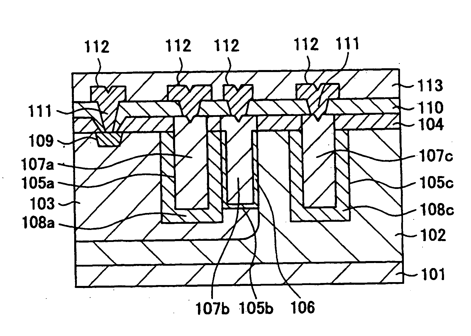
[0030]FIG. 1(a) is a sectional view illustrating a trench type LDMOS, that is, a first embodiment of a semiconductor device according to the invention. With the present embodiment, an NMOS is described as an example. The trench type LDMOS comprises an N well layer 102 of a second conductivity type, formed on a p-type semiconductor substrate 101, that is, a substrate of a first conductivity type, a P well layer 103 of the first conductivity type, formed in the N well layer 102, a source electrode 107a, a gate electrode 107b, formed in a source trench cavity 105a, a gate trench cavity 105b, respectively, within the P well layer 103, and a drain electrode 107c formed in a drain trench cavity 105c within the N well layer 102.

[0031] Further, in order to form the source electrode and the drain electrode, an N+ diffused layer 108a which is a first heavily doped region of the second conductivity is formed around the source trench cavity 105a, and an N+ diffused layer 108c which is a second...

second embodiment

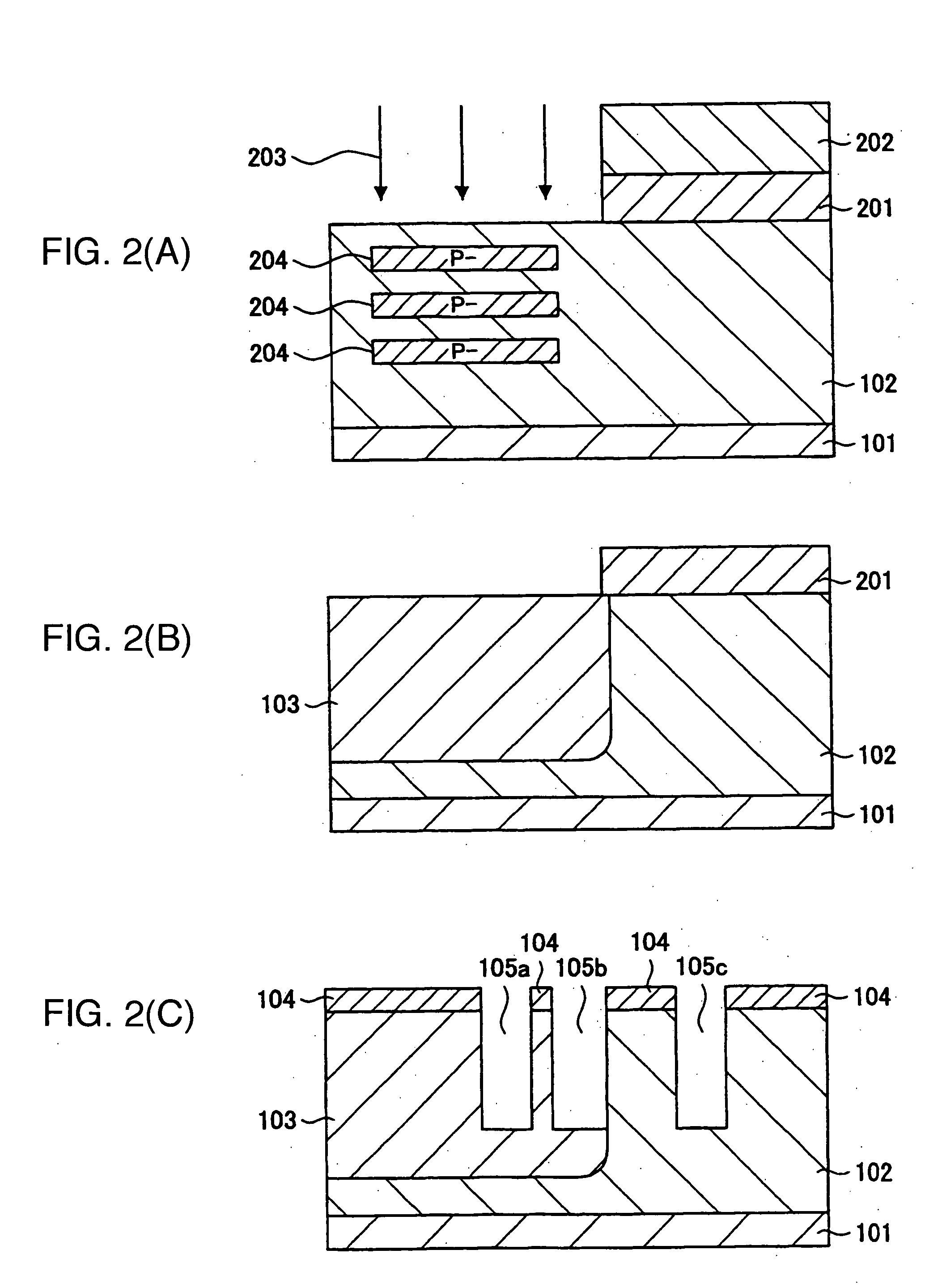
[0043] Now, a process of fabricating the n-channel trench type LDMOS according to the first embodiment is described with reference to FIGS. 2(a) through 2(f). First, the p-type semiconductor substrate 101 is prepared. For the substrate, use can be made of a silicon substrate doped with, for example, boron and formed such that sheet resistance thereof has a resistance value at about 10 to 50Ω·cm.

[0044] Subsequently, desired regions of the p-type semiconductor substrate 101 are patterned by use of the well-known photolithography, and thereafter, the N well layer 102 is formed by use of ion implantation techniques and impurity diffusion techniques. The N well layer 102 has a thickness in a range of about 5 to 10 μm. Since the voltage resistance of the LDMOS is dependent on the impurity concentration of the N well layer 102, the impurity concentration is set by taking into account a specification voltage. The impurity concentration is normally on the order of 1 to 5 E 16 cm−3.

[0045] N...

third embodiment

[0061]FIG. 3 is a sectional view illustrating a trench type LDMOS, that is, a third embodiment of a semiconductor device according to the invention. The third embodiment has a feature that an insulating oxide film layer is formed underneath the layer of the second conductivity type as described with reference to the first embodiment. That is, a SOI (Silicon On Insulator) substrate is used in place of the substrate used in the case of the first embodiment.

[0062] First, there is prepared the SOI substrate obtained by forming a polysilicon oxide film 302 as the insulating oxide film layer, on top of a p-type semiconductor substrate 301 doped with boron that is a substrate of a first conductivity type, serving as a support substrate, and further, by forming a silicon layer on the polysilicon oxide film 302. As is well known, for the SOI substrate, use may be made of any of those prepared by use of a lamination process, a doping process by implantation of oxygen ions, and so forth.

[006...


PUM


Abstract

There is provided a semiconductor device structured so as to be mounted jointly with other devices on one chip, and capable of controlling a large current in spite of a small device area while having small on-resistance, thereby enabling a high voltage resistance to be obtained. In the case of NLDMOS, the semiconductor device comprises an N well layer, formed on a p-type semiconductor substrate, a P well layer formed in the N well layer, a source electrode formed in a source trench cavity within the P well layer, a gate electrode formed in at least one of gate trench cavities within the P well layer, through the intermediary of an oxide film, and a drain electrode formed in a drain trench cavity within the N well layer, and further, N+ diffused layers are formed around the source trench cavity, the drain trench cavity, respectively.

Description

FIELD OF THE INVENTION [0001] The present invention relates to a semiconductor device, particularly, to a structure of an LDMOS (Lateral Diffusion MOS) transistor in widespread use as a power control device for a motor, relay, and so forth, and a process of fabricating the same. BACKGROUND OF THE INVENTION [0002] A conventional LDMOS device has been in widespread use as an IC device for power control that can be mounted jointly with other semiconductor devices on a chip by forming diffused layers in the lateral direction thereof. FIG. 4 shows a basic structure of a conventional n-channel LDMOS by way of example. [0003] The conventional n-channel LDMOS comprises a p-type silicon substrate 1, an N well layer 2 serving as a drain layer of the LDMOS, a P well layer 3 serving as a substrate of an N-channel MOS, a LOCOS oxide film 4 of a large thickness for the purpose of isolation and mitigation of a drain-to-gate electric field, a gate oxide film 5, a gate electrode (polysilicon film) 6...

Claims


Application Information

Patent Timeline
Patent Type & Authority Applications(United States)
IPC IPC(8): H01L21/225H01L29/786H01L21/265H01L21/336H01L27/01H01L29/10H01L29/417H01L29/423H01L29/45H01L29/76H01L29/78H01L29/94H01L31/062H01L31/113
CPCH01L21/2257H01L21/26513H01L29/1095H01L29/41766H01L29/7825H01L29/456H01L29/66674H01L29/66704H01L29/7824H01L29/4238H01L29/66696
Inventor MURAKAMI, NORIO
Owner LAPIS SEMICON CO LTD
Learn More