

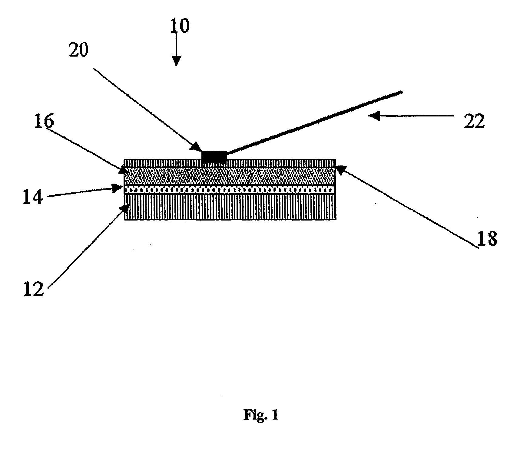
Wide band gap semiconductor composite detector plates for x-ray digital radiography
a technology of x-ray digital radiography and composite detectors, which is applied in the direction of photosensitive material auxillary/base layers, instruments, electrical equipment, etc., can solve the problems of large crystals that require long periods of growth, large crystal loss, and low sensitivity, so as to improve direct x-ray radiation-to-electrical signal conversion, the effect of low cos
- Summary
- Abstract
- Description
- Claims
- Application Information
AI Technical Summary
Benefits of technology
Problems solved by technology
Method used
Image

Examples
example 1
[0148] A 0.6 M aqueous solution of HgCl2 and a 1.2 M aqueous solution of KI were mixed quickly in a container. The Hgl2 which precipitated was washed with water, filtered and dried, the washing, filtering and drying cycle being repeated three times. The mixture was then sieved and separated into fractions by grain size. The fraction passing through the 20 micron sieve was used and microscopic inspection of that fraction showed that more than 90% of the particles had a diameter of 5 microns or less. The mercuric iodide particulates were then mixed with a 25 wt % polystyrene / toluene solution. The homogeneous mixture obtained had a weight ratio of Hgl2 to dry polystyrene of about 4.4:1.
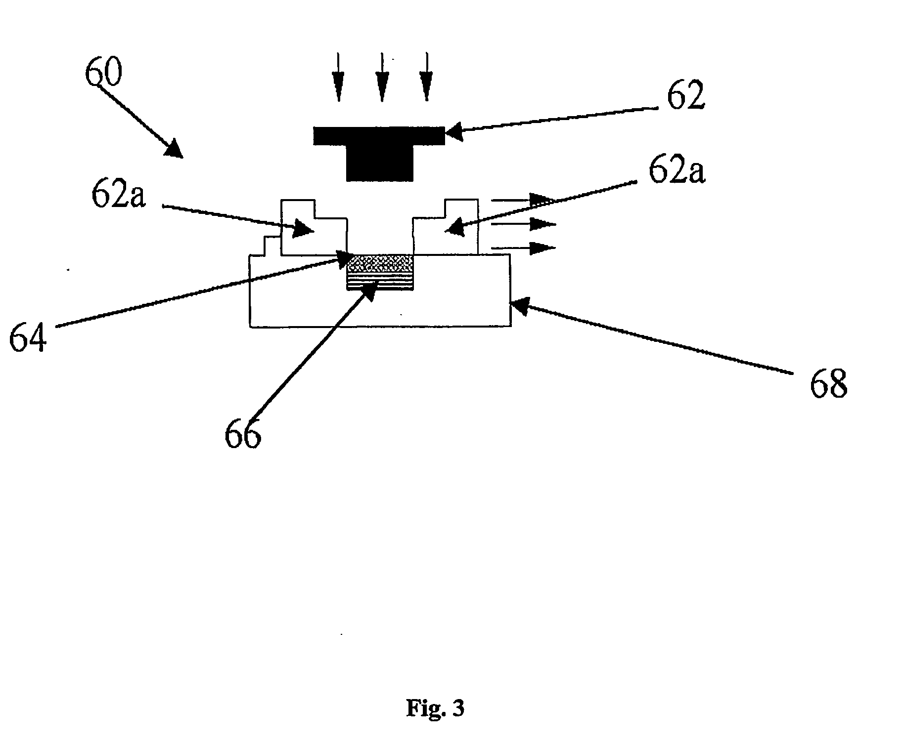
[0149] A TFT substrate was coated with indium-tin oxide (ITO) to which a thin adhesive tie layer (Humiseal® 1B12) was applied. The ITO layer served as the bottom pixel electrode. The pixels had a size of about 100×100 microns, each separated by about 10 microns. The adhesive tie layer had a thickness of...
example 2
[0152] As in Example 1, but instead of placing the Hgl2 / polystyrene mixture in a die press, the mixture was placed in a doctor blade assembly similar to the one shown in FIG. 4.
example 3
[0153] As in Example 1, but instead of placing the Hgl2 / polystyrene mixture in a die press, the mixture was placed on a screen printing apparatus similar to the one shown in FIG. 5.
PUM
 Abstract
Description
Claims
Application Information