Semiconductor thin film decomposing method, decomposed semiconductor thin film, decomposed semiconductor thin film evaluation method, thin film transistor made of decomposed semiconductor thin film, and image display device having circuit constituted of thin film transistors

a semiconductor and thin film technology, applied in the field of semiconductor thin film decomposing method, can solve the problems of irregular grain size and protrusion height, so as to reduce the protrusion effect and long crystallization process time

Inactive Publication Date: 2005-06-30
PANASONIC LIQUID CRYSTAL DISPLAY CO LTD +1
View PDF4 Cites 39 Cited by
  • Summary
  • Abstract
  • Description
  • Claims
  • Application Information

AI Technical Summary

Benefits of technology

[0019] The method of irradiating a laser beam at a plurality of energy densities to an amorphous silicon semiconductor thin film in order to reduce protrusions to be formed on a surface of a polysilicon semiconductor thin film formed by crystallizing the amorphous silicon semiconductor thin film has the disadvantage of a long crystallizing process time because a large number of scanning times at each energy density of an irradiated laser beam. It also has the disadvantage that the protrusion reduction effect by a plurality of superposed scans at a different scanning pitch becomes irregular on a substrate (on a semiconductor thin film formed on a substrate such as a glass substrate, this being applicable in the following description). These disadvantages will be described with reference to the accompanying drawings.

Problems solved by technology

The method of irradiating a laser beam at a plurality of energy densities to an amorphous silicon semiconductor thin film in order to reduce protrusions to be formed on a surface of a polysilicon semiconductor thin film formed by crystallizing the amorphous silicon semiconductor thin film has the disadvantage of a long crystallizing process time because a large number of scanning times at each energy density of an irradiated laser beam.
It also has the disadvantage that the protrusion reduction effect by a plurality of superposed scans at a different scanning pitch becomes irregular on a substrate (on a semiconductor thin film formed on a substrate such as a glass substrate, this being applicable in the following description).
Even crystallization is performed by a method providing a larger grain size and reducing protrusions, the grain size and protrusion height do not always satisfy the management standards because there are a fluctuation of a laser output with time and an in-plane variation of an amorphous semiconductor thin film thickness.

Method used


Image

  • Semiconductor thin film decomposing method, decomposed semiconductor thin film, decomposed semiconductor thin film evaluation method, thin film transistor made of decomposed semiconductor thin film, and image display device having circuit constituted of thin film transistors
  • Semiconductor thin film decomposing method, decomposed semiconductor thin film, decomposed semiconductor thin film evaluation method, thin film transistor made of decomposed semiconductor thin film, and image display device having circuit constituted of thin film transistors
  • Semiconductor thin film decomposing method, decomposed semiconductor thin film, decomposed semiconductor thin film evaluation method, thin film transistor made of decomposed semiconductor thin film, and image display device having circuit constituted of thin film transistors

Examples


first embodiment

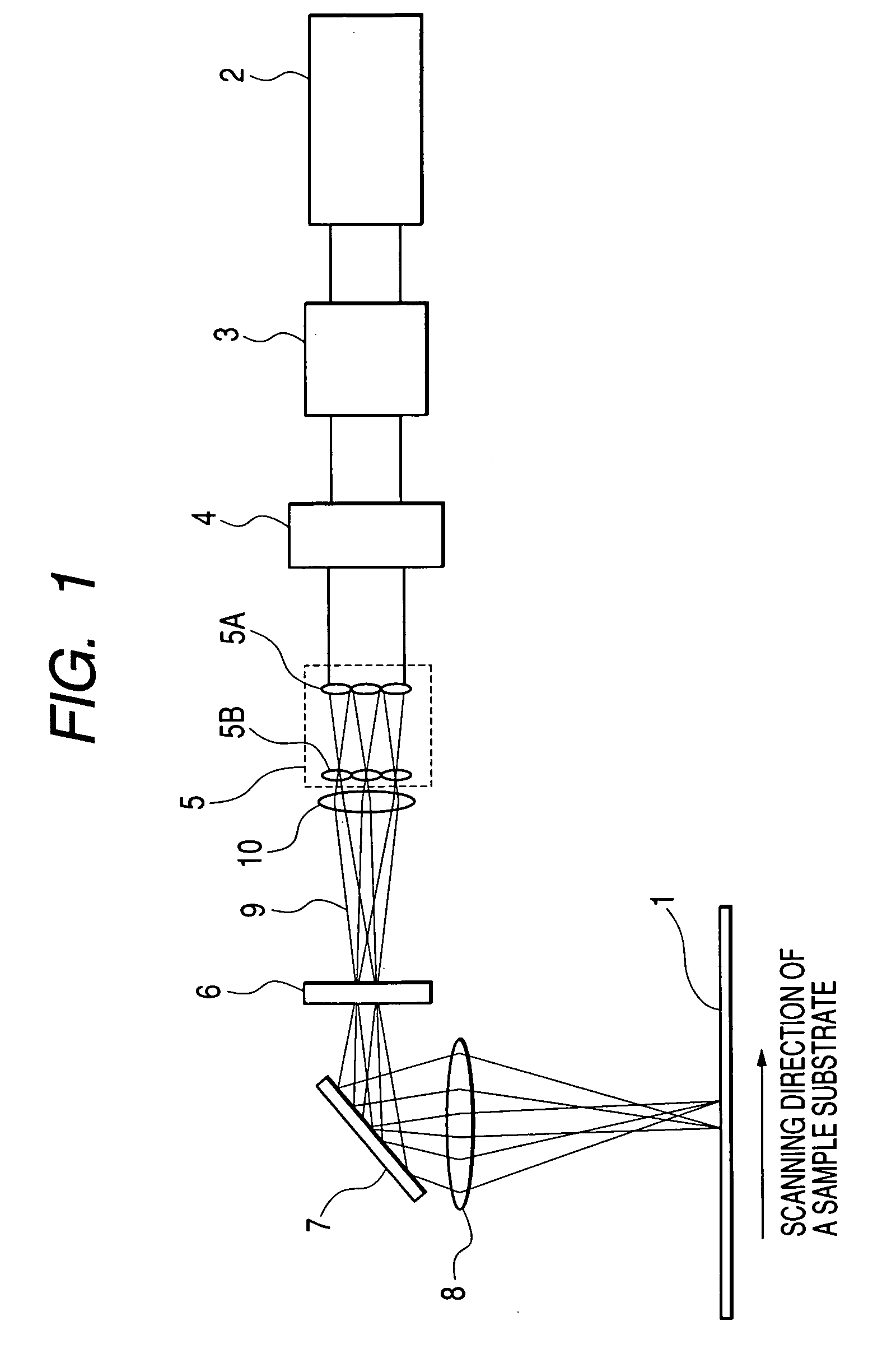
[0074]FIG. 1 is a schematic diagram showing an example of an optical system of a laser annealing apparatus realizing a semiconductor decomposition method of the present invention. In this embodiment, a transmittance distribution control filter of the present invention is applied to an excimer laser annealing apparatus used generally. Referring to FIG. 1, a laser source 2 is a STEEL1000 type XeCl excimer laser source manufactured by Lambda Physik. The wavelength of an output laser beam is 308 nm, a pulse time duration is about 27 ns, a repetition frequency is 300 Hz and a pulse energy is 1 J / pulse. This laser annealing apparatus was manufactured by Japan Steel Works, Ltd. A laser beam shaped to a line beam having a long axis length of 365 mm and a short axis length of 400 μm is irradiated to a substrate, by using a long axis homogenizer optical system 4 and a short axis homogenizer optical system 5 manufactured by MicroLas and a cylindrical lens 10, a cylindrical lens 8 and a mirror ...

second embodiment

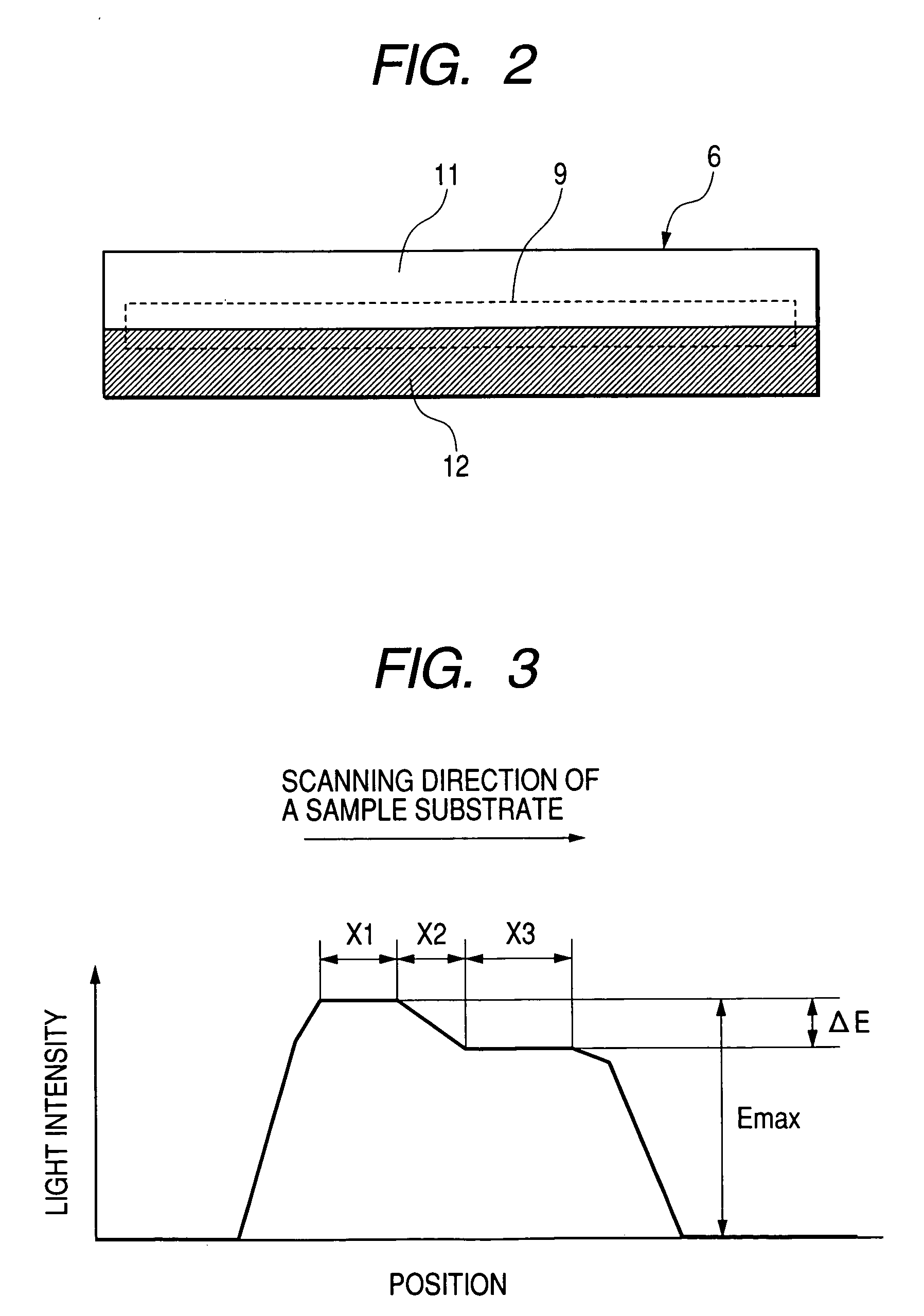
[0081] Next, with reference to FIGS. 5 and 6, the second embodiment will be described. FIG. 5 is a schematic diagram showing another example of the optical system of the laser annealing apparatus realizing the semiconductor manufacture method of the present invention. FIG. 6 is a schematic diagram showing an example of the structure of a transmittance distribution filter 6 shown in FIG. 5. This embodiment has fundamentally the same structure constituted of the laser source 2 and laser annealing apparatus of the first embodiment described with reference to FIG. 1. Different points of the second embodiment from the first embodiment reside in that the transmittance distribution filter 16 is disposed just in front of a short axis homogenizer 5 and that the transmittance distribution of the transmittance distribution filter 16 has a shape of stripes so as to control the intensity distribution in respective lenses of the cylindrical lens array in the short axis homogenizer 5 as shown in F...

third embodiment

[0083] In this embodiment, the transmittance distribution filter is applied to the crystallization method using a phase shift stripe mask. FIG. 7 is a schematic diagram showing another example of the optical system of the leaser annealing apparatus using the phase shift stripe method realizing the semiconductor manufacture method of the present invention. This embodiment uses a general excimer laser annealing apparatus using a line beam of the above-described first and second embodiments. The position of the transmittance distribution filter 6 may be the same as that shown in FIG. 1 or 5. In FIG. 7, the position of the transmittance distribution filter is the same as that shown in FIG. 1. In this embodiment, a phase stripe mask 41 is disposed near a substrate 1. The mask may be disposed on the first order focussing plane.

[0084]FIG. 8 is a diagram illustrating a method of crystallizing a silicon semiconductor thin film by using a phase shift stripe mask. As shown in FIG. 8, the phas...


PUM

PropertyMeasurementUnit
grain boundary sizeaaaaaaaaaa
heightsaaaaaaaaaa

Abstract

A surface roughness of a polycrystalline semiconductor film to be formed by a laser annealing method is reduced. A transmittance distribution filter is disposed at the optical system of a laser annealing apparatus. The transmittance distribution filter controls an irradiation light intensity distribution along a scanning direction of a substrate formed with an amorphous silicon semiconductor thin film to have a distribution having an energy part equal to or higher than a fine crystal threshold on a high energy light intensity side and an energy part for melting and combining only a surface layer. This transmittance distribution filter is applied to an excimer laser annealing method, a phase shift stripe method or an SLS method respectively using a general line beam to thereby reduce the height of protrusions on a polycrystalline surface.

Description

[0001] The present application claims priority from Japanese application JP2003-364539 filed on Oct. 24, 2003, the content of which is hereby incorporated by reference into this application. BACKGROUND OF THE INVENTION [0002] 1. Field of the Invention [0003] The present invention relates to a semiconductor thin film decomposing method of decomposing an amorphous semiconductor thin film into a polycrystalline semiconductor thin film, a decomposed semiconductor thin film evaluation method, a thin film transistor made of a decomposed semiconductor thin film, and a semiconductor device including a flat panel type image display device having a circuit constituted of thin film transistors. [0004] 2. Description of the Related Art [0005] A flat panel type image display device such as a liquid crystal display device has a pixel circuit and a drive circuit fabricated in a semiconductor thin film formed on an insulating substrate (hereinafter, also called simply a substrate), preferably a gla...

Claims


Application Information

Patent Timeline
Patent Type & Authority Applications(United States)
IPC IPC(8): G02F1/1368B23K26/073H01L21/20H01L21/268H01L21/324H01L21/336H01L21/77H01L27/12H01L29/786
CPCB23K26/0656B23K26/0738H01L27/1285H01L29/66757H01L29/78675H01L21/2026B23K26/066H01L21/02686H01L21/02502H01L21/02488H01L21/02678H01L21/02422H01L21/02532H01L21/02691H01L21/20H01L21/324
Inventor TAKEDA, KAZUOSATO, TAKESHISAITO, MASAKAZUGOTOH, JUN
Owner PANASONIC LIQUID CRYSTAL DISPLAY CO LTD
Why Eureka
Try Eureka