

Process for preparing low dielectric constant material
a dielectric constant and material technology, applied in the field of low dielectric constant material preparation, can solve the problems of deterioration in reliability of wiring and device, temperature rise of semiconductor devices, propagation delay of signals on wiring, etc., and achieve the effects of high reliability of devices, excellent mechanical strength and easy production of semiconductor devices
- Summary
- Abstract
- Description
- Claims
- Application Information
AI Technical Summary
Benefits of technology
Problems solved by technology
Method used
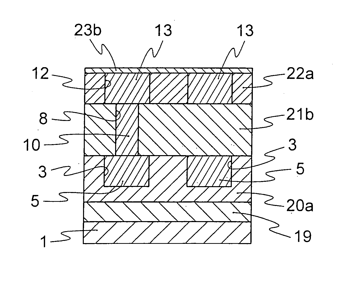
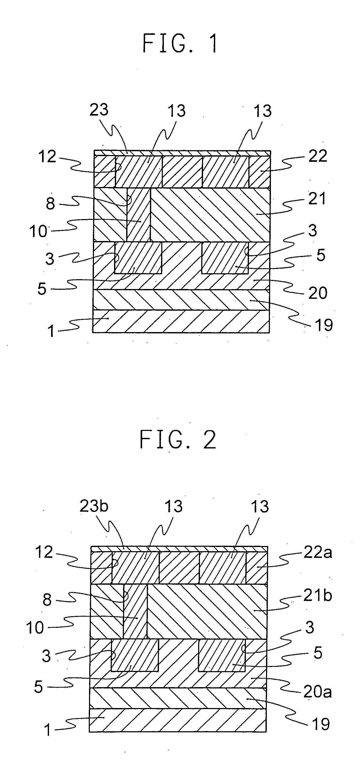
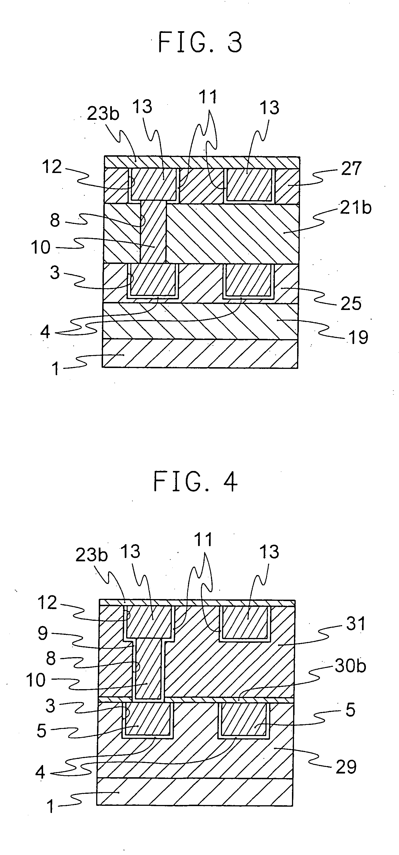
Image

Examples
example 1
[0085] Soluble poly(B-trimethylborazilene) was synthesized according to Fazen et al's method disclosed in Fazen et al., Chem. Mater., Vol. 7, p 1942, 1995.
[0086] Tetraglyme was used as a solvent, and B-trimethylborazine was heated in an Ar gas at 220° C. for two weeks with stirring and degassing to give a highly viscous liquid. The liquid was evaporated to give a white powder of a low dielectric constant material according to the present invention.
[0087] This material had a chemical structure shown by the following formula (117):
and had an average molecular weight (Mn) of about 7,500.
[0088] The obtained low dielectric constant material was dissolved in acetone and coated by spin coating method onto a quartz plate on which gold was deposited to form a counter electrode. The coated film was then dried at 100° C. for 10 minutes and heated at 400° C. for 10 minutes to give an insulating film according to the present invention. The thus heat-treated film was made of a partially cro...
example 2
[0089] Synthesis of soluble poly(B-triethylborzilene) was carried out in the same manner as Example 1.
[0090] Tetraglyme was used as a solvent, and B-triethylborazine was heated in an Ar gas at 220° C. for two weeks with stirring and degassing to give a highly viscous liquid. The liquid was evaporated to give a white powder of a low dielectric constant material according to the present invention.
[0091] This material had a chemical structure shown by the following formula (118):
and had an average molecular weight (Mn) of about 5,500.
[0092] An insulating film was formed from the obtained low dielectric constant material by conducting the spin coating in the same manner as in Example 1 and drying at 100° C. for 10 minutes. Gold was then deposited onto the insulating film as a main electrode.
example 3
[0093] A white powder of poly(methylborazinylamine) was prepared according to Narula et al's method disclosed in C. K. Narula, R. Schaeffer, R. T. Paine, A. K. Datye and W. F. Hammetter, J. Am. Chem. Soc., Vol. 109, p 5556 (1987). The thus obtained low dielectric constant material was dispersed into acetone, and the dispersion was coated by spin coating and dried at 100° C. for 10 minutes in the same manner as in Example 1 to give an insulating film. Gold was then deposited thereon as a main electrode.
PUM
| Property | Measurement | Unit |
|---|---|---|
| dielectric constant | aaaaa | aaaaa |
| dielectric constant | aaaaa | aaaaa |
| dielectric constant | aaaaa | aaaaa |
Abstract
Description
Claims
Application Information