Method of producing an electron emission device, method of producing an electron source, method of producing an image display device, and method of driving an electron emission device

Inactive Publication Date: 2005-09-15
CANON KK
View PDF9 Cites 20 Cited by
  • Summary
  • Abstract
  • Description
  • Claims
  • Application Information

AI Technical Summary

Benefits of technology

[0032] The production method according to the present invention in the first or the second aspect makes it possible to produce a high-efficiency electron emission device having a simple structure, capable of being driven by a low driving voltage, capable of well controlling the electron beam diameter, and capable of stably emitting electrons in low strength electric fields. T

Problems solved by technology

Any change in the characteristics of the electron emission film during the production process makes it difficult to achieve the expected electron emission performance.
Since electron emission characteristics of electron emissi

Method used


Image

  • Method of producing an electron emission device, method of producing an electron source, method of producing an image display device, and method of driving an electron emission device
  • Method of producing an electron emission device, method of producing an electron source, method of producing an image display device, and method of driving an electron emission device
  • Method of producing an electron emission device, method of producing an electron source, method of producing an image display device, and method of driving an electron emission device

Examples


example 1

[0226] Specific examples based on the production method shown in FIGS. 8 and 9 are described.

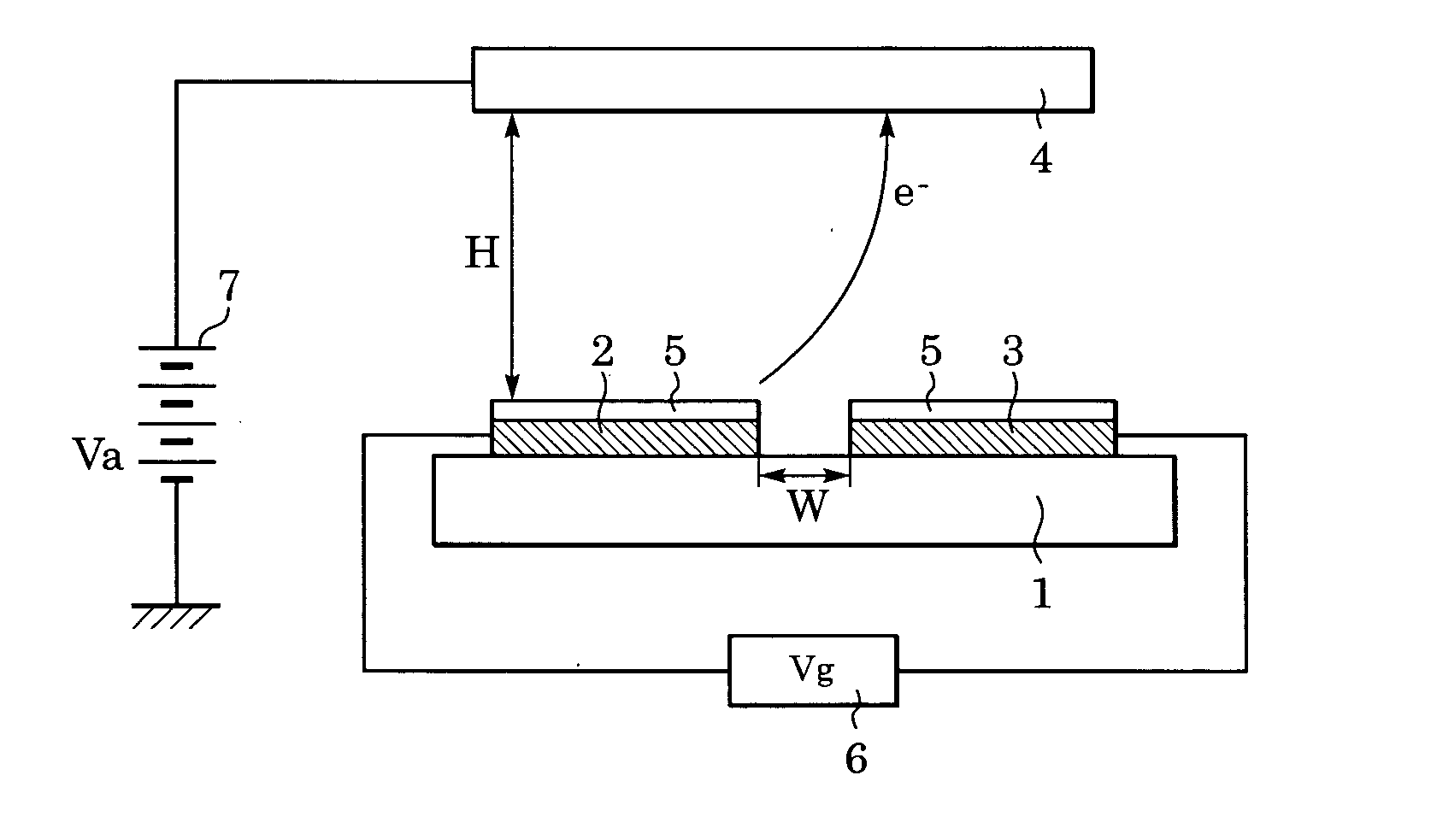
[0227] An electron emission device including a carbon layer 5 with a dipole layer 11 shown in FIG. 6 was produced.

Step 1

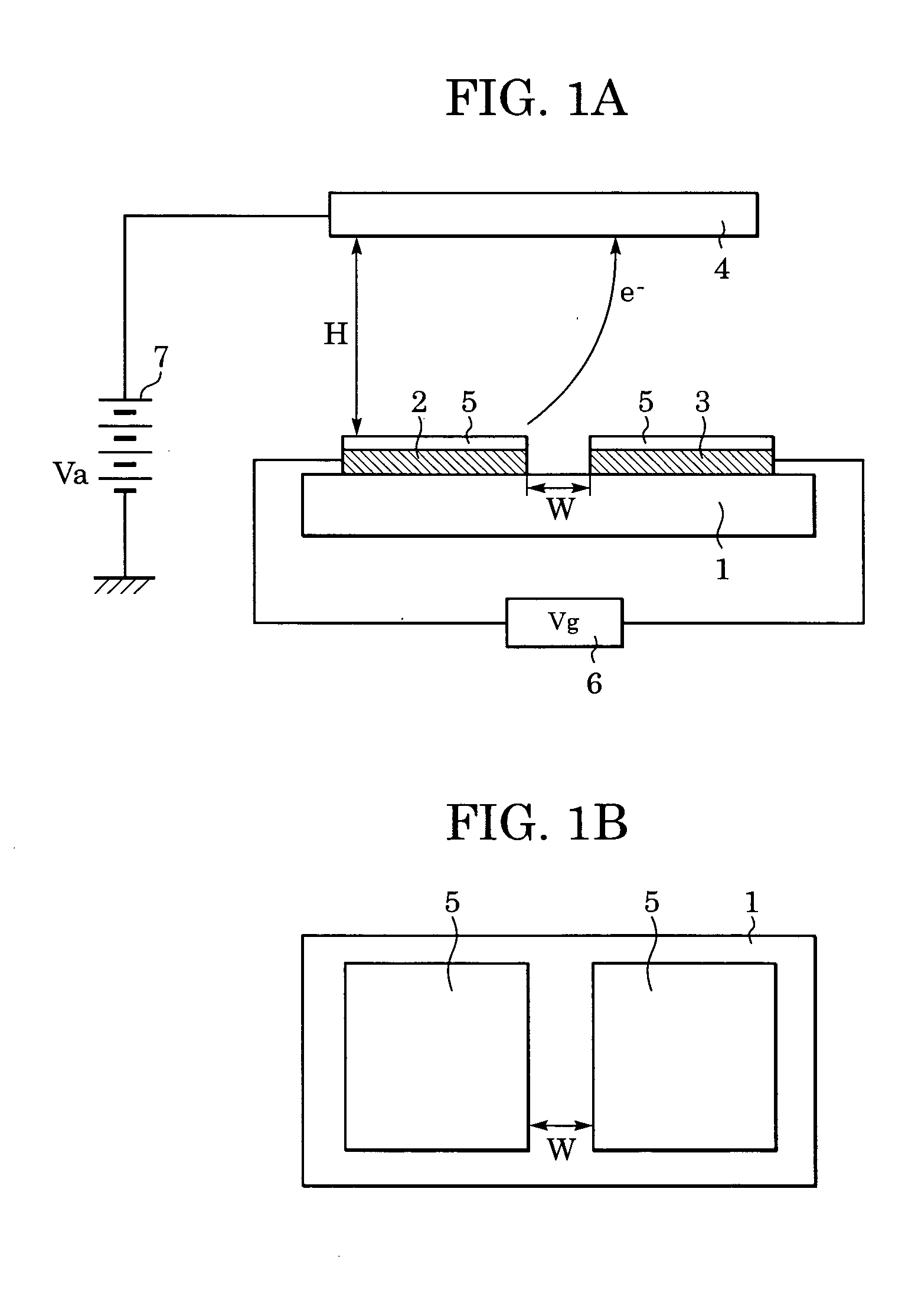
[0228] First, a substrate 1 of quartz glass was prepared. After the substrate 1 was cleaned well, a conductive film 31 to be further formed into a cathode electrode 2 and the gate electrode 3 was formed by sputtering TiN on the substrate 1 to a thickness of 100 nm (FIG. 8A).

Step 2

[0229] A carbon layer 5 with a thickness of 4 nm was then formed by means of sputtering using graphite as a target in an ambient of argon. The resistivity of the obtained carbon layer 5 was 1×10¹¹ Ω·cm (FIG. 8B).

Step 3

[0230] A resist mask 33 with a thickness of 1 μm was produced by means of a photolithographic process such that W became 1 μm (FIG. 8C).

Step 4

[0231] Subsequently, the carbon layer and the TiN electrode were successively dry-etched. To completely etch the TiN electrode, ov...

example 2

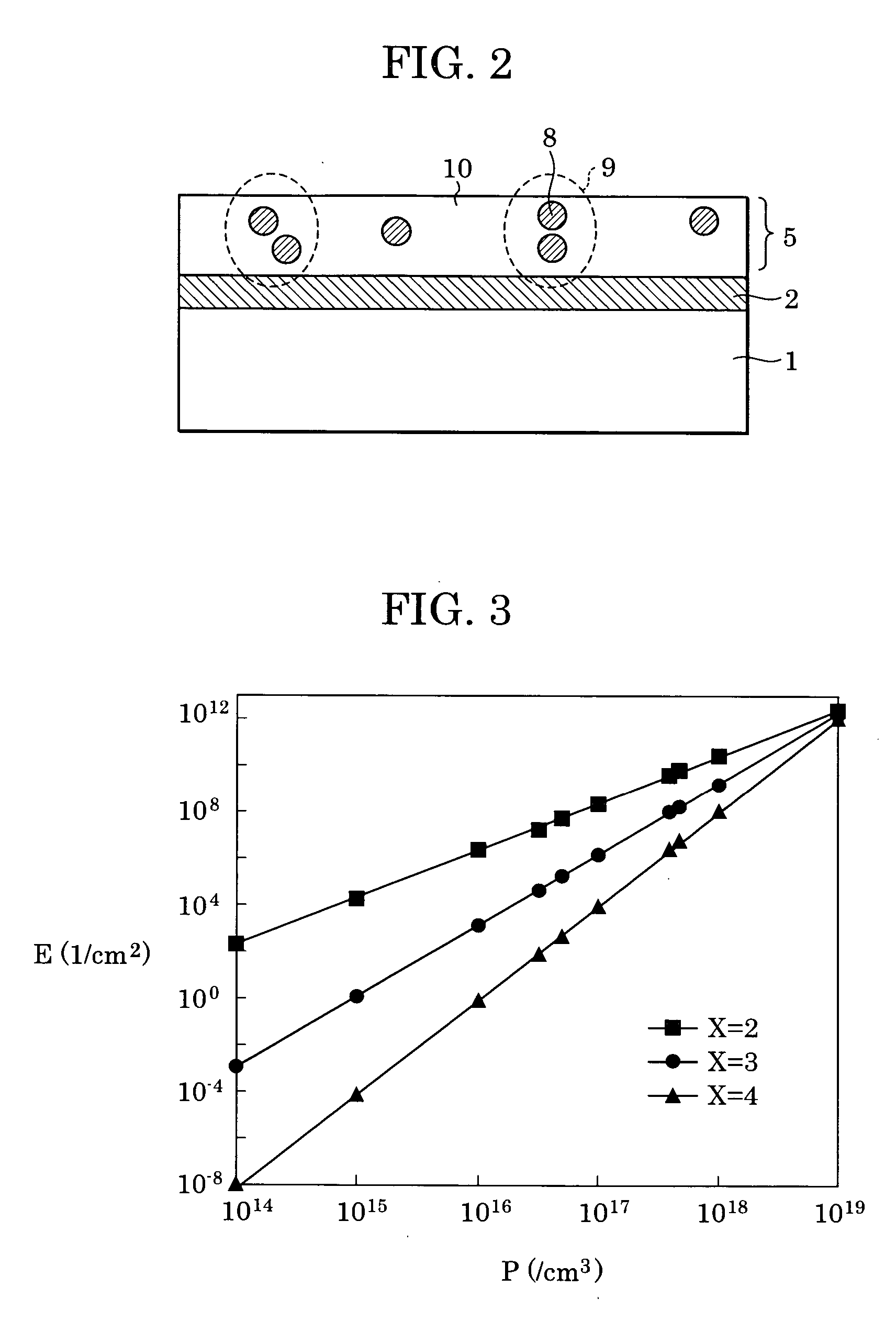
[0248] In Example 2, the carbon film shown in FIG. 2 was used.

Step 1

[0249] Step 1 was performed in a similar manner to step 1 of Example 1.

Step 2

[0250] Subsequently, to form the carbon layer 5, a DLC film with a thickness of 30 nm was deposited using an HFCVD (hot-filament chemical vapor deposition) method. The resistivity of the obtained DLC film was as high as 1×10¹² Ω·cm. The growth conditions employed are as follows: [0251] Gas: CH4 [0252] Substrate bias: −50 V [0253] Gas pressure: 267 mPa [0254] Substrate temperature: Room temperature [0255] Filament: Tungsten [0256] Filament temperature: 2100° C.

Subsequently, the carbon layer 5 was doped with cobalt by implanting cobalt into the carbon layer 5 with energy of 25 keV to a dose of 3×1016 cm−2.

Steps 3 to 5

[0257] Steps 3 to 5 were performed in a similar manner as in Example 1, except that dry etching conditions were adjusted depending on the film thickness of the carbon film.

[0258] Subsequently, using a lamp, heat treat...

example 3

[0272] An electron emission device having a structure shown in FIGS. 15A and 15B was produced.

Step 1

[0273] First, a substrate 1 of quartz glass was prepared. After the substrate 1 was cleaned well, a film of Ta with a thickness of 500 nm was deposited by means of sputtering to form a cathode electrode 2.

Step 2

[0274] Thereafter, an insulating film 61 was formed by depositing a SiO2 film with a thickness (h) of 1 μm and then a gate electrode 3 was formed by depositing a Ta film with a thickness of 100 nm.

Step 3

[0275] Subsequently, a mask pattern was formed using a photolithography technique. More specifically, a positive photoresist (AZ1500 available from Clariant Corporation) was spin-coated and then exposed to a photomask pattern. Development was then performed thereby forming the mask pattern.

Step 4

[0276] By using the mask pattern as an etching mask, the gate electrode 3 of Ta was dry-etched using CF4 gas and then the SiO2 film 17 was etched using buffered hydrofluoric ...


PUM


Abstract

A method of producing an electron emission device having a low threshold electric field needed to emit electrons without unintentional electron emission includes a first step of preparing a first conductive film, second conductive film, and a material which constitutes an electron emission part connected to the first conductive film, and a second step of setting a threshold electric field strength, which is needed to start electron emission in a situation where a higher electric potential is applied to the first conductive film than that applied to the second conductive film, to a value greater than a threshold electric field strength, which is needed to start electron emission in a situation where a higher electric potential is applied to the second conductive film than that applied to the first conductive film.

Description

BACKGROUND OF THE INVENTION [0001] 1. Field of the Invention [0002] The present invention relates to a method of producing an electron emission device using an electron emission film, and a method of producing an image display device having a plurality of electron emission devices. [0003] 2. Description of the Related Art [0004] Electron emission devices can be classified into three types: a field emission (FE) type, an MIM type, and a surface conduction type. Basically, in any type, the electron emission device includes a cathode electrode including an electron emission part and a control electrode for controlling emission of electrons from the electron emission part or controlling electrons emitted from the electron emission part. [0005] Electron emission devices of the FE type can be further classified into two types: a type (Spindt type) in which an opening is formed in a control electrode and a cathode electrode made of metal and having a sharp tip (formed in a cone shape) is d...

Claims


Application Information

Patent Timeline
IPC IPC(8): H01J9/02H01J9/00H01J9/44
CPCH01J1/316H01J31/127H01J9/027A63H27/04A63H27/12A63H29/18G09B19/10
Inventor NISHIMURA, MICHIYO
Owner CANON KK
Why Eureka
Try Eureka