Semiconductor device

a semiconductor device and semiconductor technology, applied in semiconductor devices, semiconductor/solid-state device details, electrical apparatus, etc., can solve the problems of schottky diodes, hetero-bipolar transistors (hbts), and non-uniform resistivity of the surface,

Active Publication Date: 2005-09-22
PANASONIC CORP
View PDF5 Cites 17 Cited by
  • Summary
  • Abstract
  • Description
  • Claims
  • Application Information

AI Technical Summary

Benefits of technology

[0018] In the inventive device, the device formation region preferably includes a channel layer in which electrons move; the first electrode is preferably a gate electrode; the second electrode is preferably a drain electrode; the semiconductor device preferably further includes a source electrode formed in a position that opposes the drain electrode with the gate electrode interposed; and the semiconductor device preferably operates as a field effect transistor, and the semi-insulating film preferably covers a portion of the surface of the device formation region, which is located between the gate and drain electrodes. By forming the semiconductor device having this structure, a high-voltage filed effect transistor is obtained.
[0019] In this case, the semi-insulating film preferably has a resistivity that is lower than that of silicon nitride and that makes a time constant, which is the product of a value of capacitance between the drain and source electrodes and a value of resistance occurring between th

Problems solved by technology

However, crystal defects or the like, occurring during a crystal growth step or other fabrication process steps, are present on the surface of the undoped AlGaAs layer 103, causing the resistivity of the surface to be nonuniform.
This results i

Method used


Image

  • Semiconductor device
  • Semiconductor device
  • Semiconductor device

Examples


first embodiment

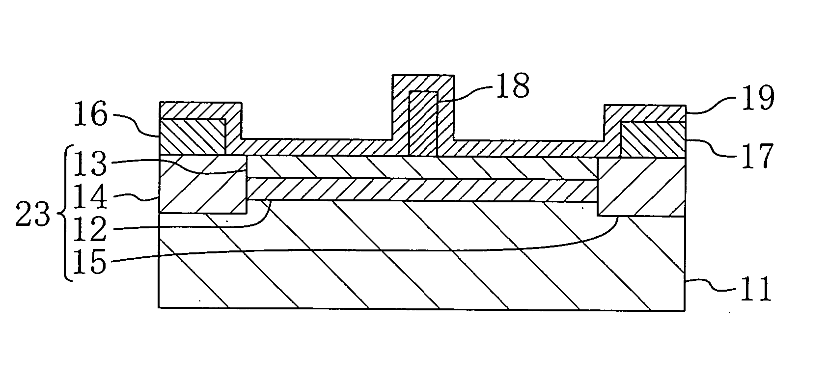
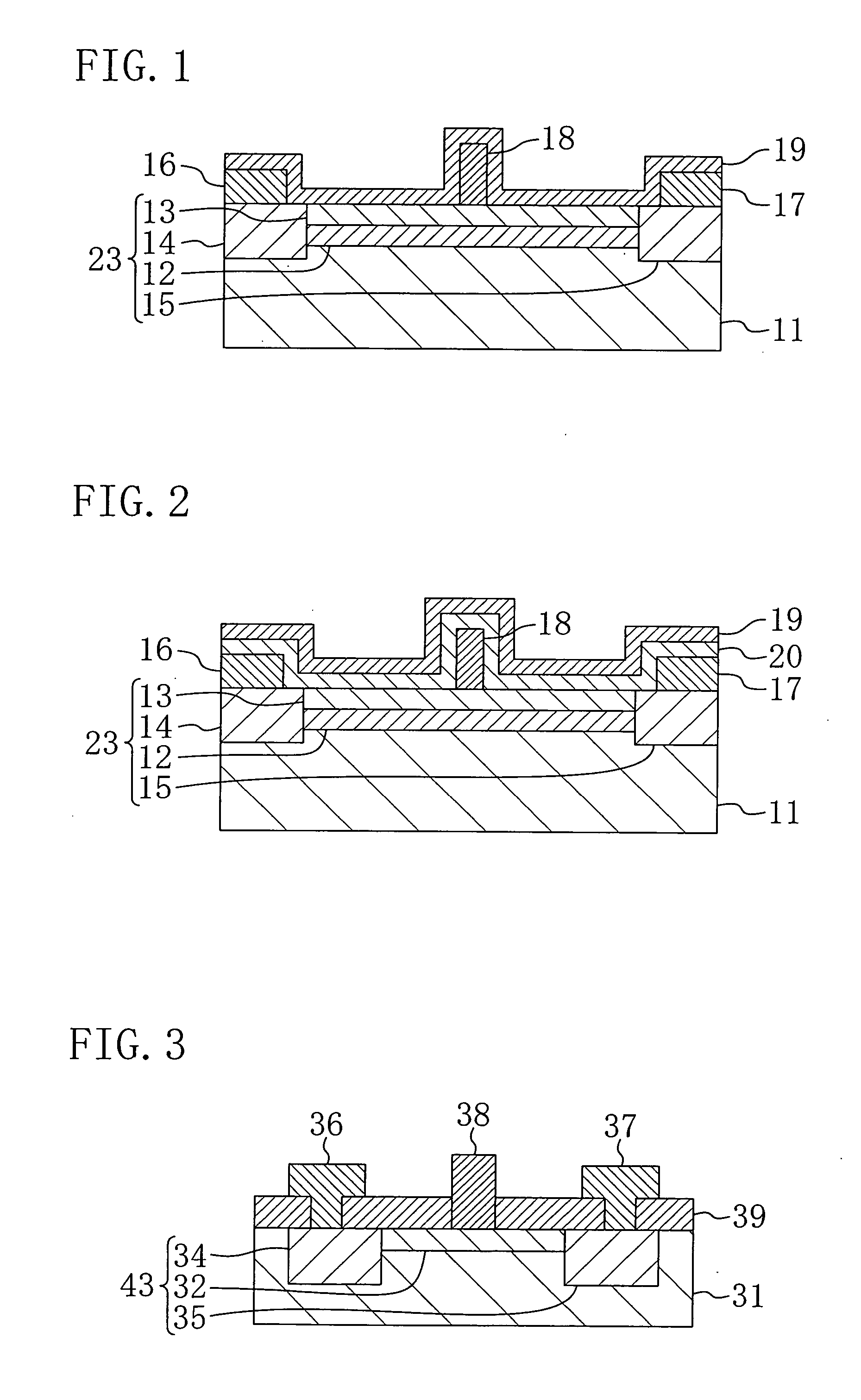
[0036] A semiconductor device according to a first embodiment of the present invention will be described with reference to the accompanying drawings. FIG. 1 illustrates a cross-sectional structure of the semiconductor device of this embodiment. As shown in FIG. 1, the semiconductor device of this embodiment is a metal semiconductor field effect transistor (MESFET). In the semiconductor device, a device formation region 23 is formed consisting of: an n-type GaAs channel layer 12 formed on a semi-insulating GaAs substrate 11; an undoped AlGaAs layer 13 formed on the channel layer 12; and source and drain regions 14 and 15, which are high carrier concentration regions formed with both sides of the channel layer 12 and AlGaAs layer 13 interposed therebetween. A gate electrode 18 is formed on the AlGaAs layer 13, while source and drain electrodes 16 and 17 are formed with the gate electrode 18 sandwiched therebetween. The source and drain electrodes 16 and 17 are formed on the source and...

second embodiment

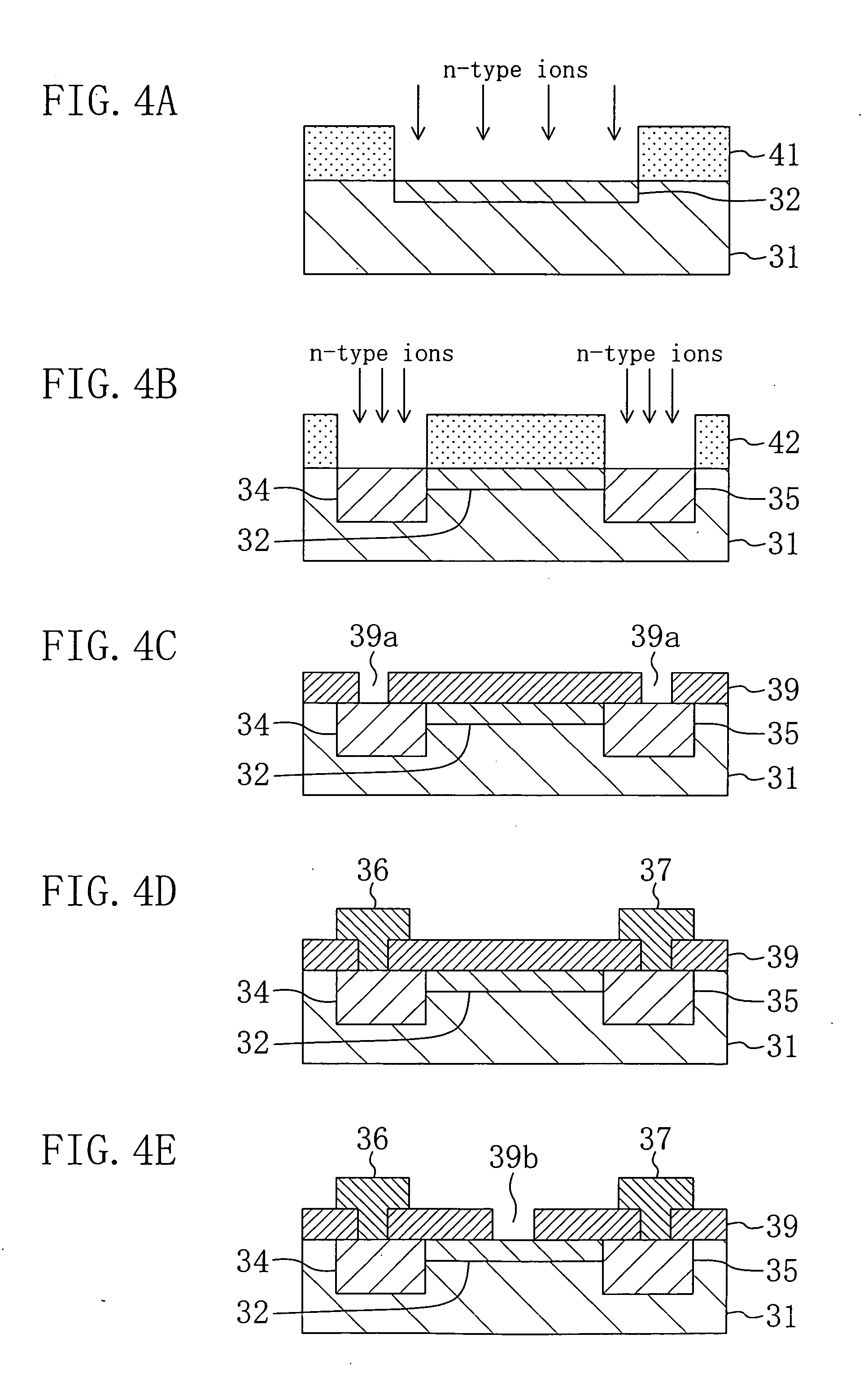
[0050] Hereinafter, a semiconductor device according to a second embodiment of the present invention will be described with reference to the accompanying figures. FIG. 3 illustrates a cross-sectional structure of the semiconductor device of this embodiment. As shown in FIG. 3, the semiconductor device of this embodiment is a MESFET that has a semiconductor region formed by implanting ions into a semiconductor substrate. A device formation region 43 is formed in a near-surface portion of a semi-insulating GaAs substrate 31 having a thickness of 500 μm. The device formation region 43 is composed of high concentration n-type source and drain regions 34 and 35 formed spaced apart from each other, and an n-type region 32 formed between the source and drain regions 34 and 35. On the GaAs substrate 31 that includes the device formation region 43, a 200-nm-thick BCN film 39 is formed.

[0051] Source and drain electrodes 36 and 37 are formed on portions of the surface of the BCN film 39 which...

third embodiment

[0060] Hereinafter, a semiconductor device according to a third embodiment of the present invention will be described with reference to the accompanying figures. FIG. 5 illustrates a cross-sectional structure of the semiconductor device of this embodiment. As shown in FIG. 5, the semiconductor device of this embodiment is a high electron mobility transistor (HEMT), in which a device formation region 63 made of semiconductor layers is formed on a sapphire substrate 51 having a thickness of 500 μm. The device formation region 63 is composed of a buffer layer 52, a channel layer 53, and an electron supply layer 54. The buffer layer 52 is made of aluminum nitride (AlN) and having a thickness of 500 nm. The channel layer 53 formed on the buffer layer 52 is made of a 2-μm-thick undoped GaN film. The electron supply layer 54 formed on the channel layer 53 is made of a 25-nm-thick undoped Al0.25Ga0.75N film. A high-concentration two-dimensional electron gas (2DEG) is formed in the channel l...


PUM


Abstract

The semiconductor device of the present invention includes a device formation region formed on a substrate and including at least one semiconductor region, and a first electrode and a second electrode formed spaced apart from each other on the device formation region. A semi-insulating film is formed to cover the surface of a portion of the semiconductor region, which portion is located between the first and second electrodes and in which portion a depletion layer extends when a reverse bias is applied between the first and second electrodes.

Description

CROSS-REFERENCE TO RELATED APPLICATION [0001] This application claims priority under 35 U.S.C. §119 on Patent Application No. 2004-082277 filed in Japan on Mar. 22, 2004, the entire contents of which are hereby incorporated by reference. BACKGROUND OF THE INVENTION [0002] The present invention relates to semiconductor devices, and more particularly, field effect transistors, bipolar transistors, diodes and the like that are required to have a high breakdown voltage. [0003] A MESFET (metal-semiconductor field effect transistor) is one of semiconductor devices in which compound semiconductors such as gallium arsenide (GaAs), indium phosphide (InP), and gallium nitride (GaN) are used. A MESFET has a Schottky junction in which a metal gate electrode is formed directly on a semiconductor layer, and the size of a depletion layer formed in the semiconductor layer due to the Schottky junction is made to change according to a voltage applied to the gate electrode, thereby controlling a curre...

Claims


Application Information

Patent Timeline
IPC IPC(8): H01L21/338H01L29/732H01L29/812
CPCH01L29/812H01L29/66871
Inventor YANAGIHARA, MANABUUEDA, DAISUKE
Owner PANASONIC CORP
Why Eureka
Try Eureka