Ceramic thin film on various substrates, and process for producing same

a technology of ceramic thin film and substrate, applied in the direction of crystal growth process, chemical vapor deposition coating, coating, etc., can solve the problems of contaminated film, increased disorder of si—c network, increased shrinkage and outgassing phenomena,

Inactive Publication Date: 2005-11-03
SIXTRON ADVANCED MATERIALS
View PDF12 Cites 17 Cited by
  • Summary
  • Abstract
  • Description
  • Claims
  • Application Information

AI Technical Summary

Problems solved by technology

In the method of Grigoriev et al., the polymeric source already contains most of the Si—C bonds required for the formation of the SiC film; however, the molecular source is carried to the surface inside cages of solvent molecules, implicitly leading to contamination of the film, shrinking and outgassing phenomena, due to solvent evaporation and polymer cracking.
They have observed that the disorder of the Si—C network increased with using the high bias voltages during the deposition.
Under the impact of high-energy ions or substrate heating the films consisted of Sp2 C—C bonds and Si—N bonds, and the formation of Sp3 C—N bonds was difficult.

Method used


Image

  • Ceramic thin film on various substrates, and process for producing same
  • Ceramic thin film on various substrates, and process for producing same
  • Ceramic thin film on various substrates, and process for producing same

Examples


example 1

Use of Polysilanes as PA-CVD Precursors to n-type Semiconductor a-SiC.

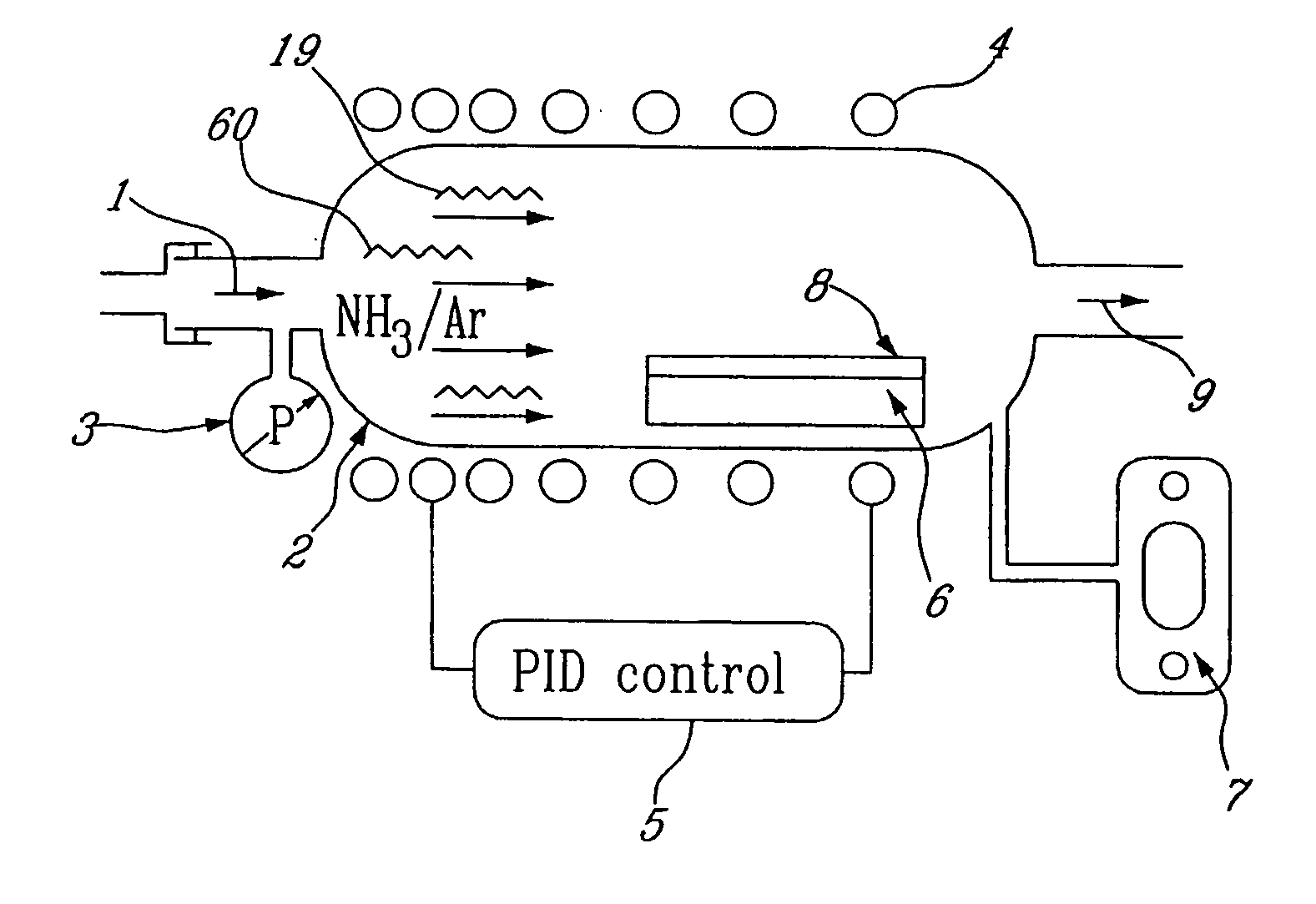
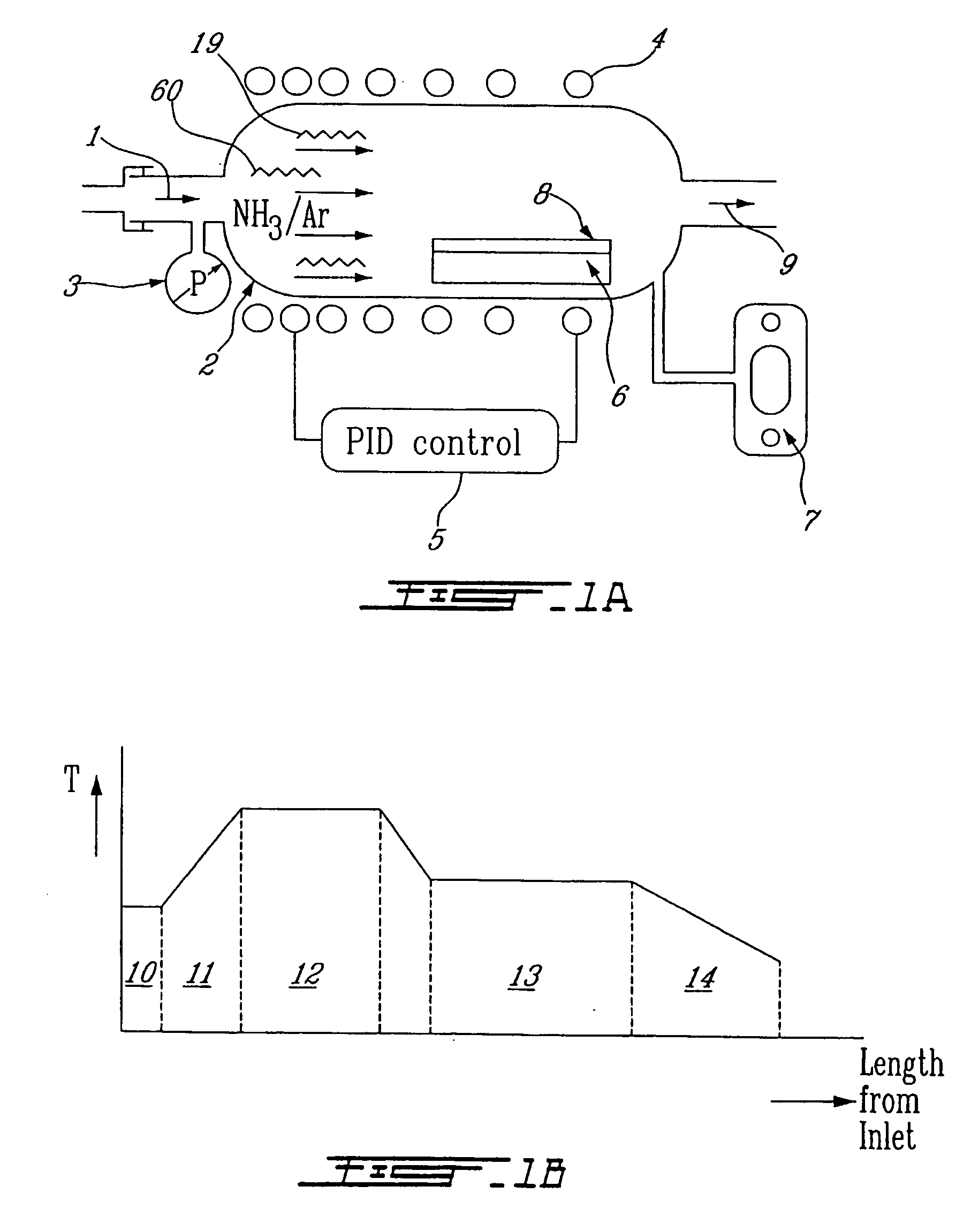
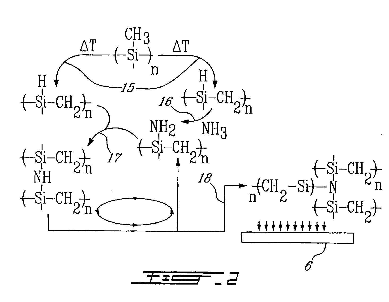
[0094] The anticeramic yield is optimized with respect to the average molecular weight and the polydispersity of the polysilane raw material. In the first step, an appropriate time-dependent temperature gradient is programmed in the furnace, so that quantitative polycarbosilane formation is promoted. Possible ranges for the gradients are 1-10 Kmin−1 and 3-50 Kcm−1 in a 2 inch / 150 cm horizontal quartz reactor (11). A second step involves polycarbosilane pyrolysis that may be coupled with a nitrogen-doping process, via a carefully monitored (flow, pressure (3), and FT-IR (7)) reaction with electronic-grade ammonia (12), at a partial pressure level of 10−6-10−1 torr in a UHP-Ar (or N2) carrier flow. The resulting polymeric gaseous species (17,18) are transported in the deposition zone (13), where they are desublimed onto the substrate (6) that can be placed in a horizontal, vertical or a tilted position, and can be ...

example 2

Use of Polysilanes as PA-CVD Precursors for the Synthesis of Thin Films of Passivating SiOxCy-glasses

[0095] Silicon oxycarbide (SiOxCy) is an amorphous metastable phase wherein the silicon atoms are bonded to oxygen and carbon simultaneously. In silicon oxycarbides, high temperature properties and chemical stability have been reported, exceeding those of ordinary vitreous silica. Silicon oxycarbide materials have also the potential for use in a variety of protective applications within the semiconductor industry. Using PA-CVD technique, silicon oxycarbides of various compositions have been deposited on highly resistive single crystal silicon wafers, using different conditions to vary the oxygen content in the films. The anticeramic yield is optimized with respect to the average molecular weight and the polydispersity of the polysilane raw material.

[0096] In the first step, an appropriate time-dependent temperature gradient is programmed in the furnace to enhance quantitative polyc...

example 3

Use of Polysilanes as PA-CVD Precursors to Dielectric or Passivating a-SixNy Thin Films

[0099] The anticeramic yield is optimized with respect to the average molecular weight and the polydispersity of the polysilane raw material. An appropriate time-dependent temperature gradient is programmed in the furnace, so that quantitative polysilazane formation is promoted. Possible ranges for the gradients are 1-5° K. min−1 and 3-50° K. cm−1 where the temperature increases (11) in a 2 inch / 150 cm horizontal quartz reactor (2). A second step involves pyrolysis of the polysilazane in the reaction zone (12) in FIG. 1 where the temperature is relatively constant. This step may be optionally followed by a transamination processes induced directly in the deposition zone (13), via a carefully monitored (flow, pressure—parameters (3) and PID temperature parameters (5) where P=1-25, I=10-250, and D=0.1-10) reaction under pure electronic-grade gaseous ammonia introduced in the temperature zone (11), ...


PUM

PropertyMeasurementUnit
temperatureaaaaaaaaaa

Abstract

The process of Polymer Assisted Chemical Vapor Deposition (PACVD) and the semiconductor, dielectric, passivating or protecting thin films produced by the process are described. A semiconductor thin film of amorphous silicon carbide is obtained through vapor deposition following desublimation of pyrolysis products of polymeric precursors in inert or active atmosphere. PA-CVD allows one or multi-layers compositions, microstructures and thicknesses to be deposited on a wide variety of substrates. The deposited thin film from desublimation is an n-type semiconductor with a low donor concentration in the range of 1014-1017 cm−3. Many devices can be fabricated by the PA-CVD method of the invention such as; solar cells; light-emitting diodes; transistors; photothyristors, as well as integrated monolithic devices on a single chip. Using this novel technique, high deposition rates can be obtained from chemically synchronized Si—C bonds redistribution in organo-polysilanes in the temperature range of about 200-450° C.

Description

FIELD OF THE INVENTION [0001] The present invention relates to a ceramic thin film which may be an amorphous silicon carbide (a-SiC) semiconductor thin film deposited on various substrates suitable for photovoltaic cells and a variety of relatively high performance low-cost electronic devices which can be easily and economically mass-manufactured. By means of Polymer-Assisted Chemical Vapor Deposition (PA-CVD), new semiconductor materials with high conversion yields can be produced at low cost. The process involves gaseous precursors from polymeric sources, which lead to chemically synchronized construction of a desirable amorphous silicon carbide structural framework with special electronic and photonic properties. BACKGROUND OF THE INVENTION [0002] Kitabatake et al., disclose in U.S. Pat. No. 6,270,573 B1, CVD and CVD-related methods of producing silicon carbide substrates, including the growing of silicon carbide film by supplying separate silicon atoms and carbon atoms on a surf...

Claims


Application Information

Patent Timeline
Patent Type & Authority Applications(United States)
IPC IPC(8): C23C16/32C23C16/46
CPCC23C16/325Y10T428/265C23C16/46Y10T428/31504
Inventor SCARLETE, MIHAIAKTIK, CETIN
Owner SIXTRON ADVANCED MATERIALS
Why Eureka
Try Eureka